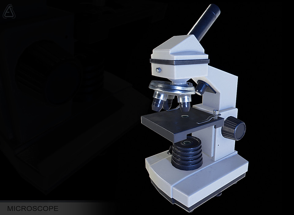
Microscope 3d scanner
3D Surface Profiler | KEYENCE America
Lineup
The VK-X3000 3D Surface Profiler uses a triple scan approach, where laser confocal scanning, focus variation, and white light interferometry measurement methods are used, so that high-accuracy measurement and analysis can be performed on any target. The VK-X3000 has a resolution of 0.01 nm and can scan areas up to 50 x 50 mm (1.97" x 1.97"), allowing for measurement of the overall shape of the target while still maintaining high-resolution for analysis of minute surface features. KEYENCE's new 3D Surface Profiler can handle any target, including those with transparent or mirrored surfaces, large height changes, or steep angles.
Catalogs Price
Features
Optical Profiler Basics
Observation
Extensive magnification coverage, ranging from optical microscopes to SEMs
- Magnification up to 28,800×
- Automatic focusing
- Observe any material
Measurement
Instant, non-contact surface scanning
- No target damage
- Accurate nano-level measurement
- Compatible with any shape or material
Analysis
Unprecedented surface characterization
- Quantification of even the most detailed shapes
- Differentiate surfaces easily
- Roughness analysis
Precise Scanning Unaffected By Material and Shape
- Accurately measure steep slopes and angled surfaces
- Best-in-class XY resolution ensures even the smallest features are captured
- No data dropout on transparent or highly-reflective surfaces
Discontinued Series
-
3D Laser Scanning Confocal Microscope
VK-X series
Discontinued
-
Color 3D Laser Scanning Microscope
VK-8700/9700 GenerationII series
Discontinued
A 3D surface profiler is a generic term used to refer to measurement systems that acquire 3D data on targets through a variety of different methods, including laser scanning confocal microscopes, interferometers, and focus variation microscopes. 3D surface profilers are commonly used for observing, measuring, and analyzing surface characteristics of various targets.
Laser confocal scanning measurement principle
Laser microscopes utilize a special optical system consisting of a light source, a light receiving element (PMT), an objective lens, a half mirror, and a pinhole in order to perform both magnified observation and surface shape analysis.
The laser light generated by the light source is concentrated at the focal point by the objective lens, with the measurement target also being placed at the focal point. The laser light then reflects from the target surface and passes through the objective lens and is focused once more. A pinhole is situated at the focal position, directly in front of the light receiving element. The focused light passes through the pinhole, and all the reflected light enters the light receiving element.
When the target is at a position that is out of focus, the laser light is not concentrated and a portion is blocked by the pinhole, reducing the amount of light that reaches the light receiving element.
Laser microscopes detect whether the sample is at the focal position according to the intensity of the reflected light that returns to the light receiving element. An optical system which incorporates a pinhole in front of the light receiving element is known as a confocal optical system, and the detection principle is known as the "confocal principle."
Laser confocal scanning methods
Some typical methods of scanning used in laser microscopes are a Galvano scanner, an acousto-optic device (AOD), or a Nipkow disk.
Galvano scanner method:
Mirrors that reflect laser light are attached to the end of servo motors. The servo motors are controlled to change the angles of the mirrors, which causes the laser to scan in the X and Y directions. While this approach can produce high data quality, scanning takes time.
Acousto-optic device (AOD) method:
This method uses an acousto-optic device, which is an acousto-optic medium made of glass to which a piezoelectric element has been attached. By applying an electric signal to this piezoelectric element, ultrasonic waves are generated. These waves diffract laser light that passes through the acousto-optic medium. While the scanning speed is fast, the data obtained is prone to distortion.
Nipkow disk method:
A disk with one or more rows of pinholes arranged in a spiral is spun, and the multiple beams of light passing through the pinholes scan across the sample surface. While this method can produce relatively high data quality, observation of samples with low reflectivity is difficult.
Additional measurement principles
In recent years, advanced 3D surface profilers that combine multiple different measurement principles have garnered increasing attention. By combining multiple measurement principles into one device, each measurement principle's weak points can be compensated for. Keyence's VK-X3000 Series 3D Surface Profiler integrates three different principles in a single unit: white light interferometry, laser confocal scanning, and focus variation. This makes it possible for a single unit to measure and analyze a variety of targets, regardless of their material, shape, or surface conditions.
Principle of white light interferometry:
White light interferometry captures 3D shape data through the observation of light interference patterns using an image sensor, such as a CMOS. Using an interference objective lens with a built-in reference mirror, white light from an LED or other light source is used to illuminate the reference mirror and the target (measurement surface). The light reflected from each object interferes with one another, and the interference pattern appears as contour lines at each half wavelength. This corresponds to the shape of the target surface with respect to the reference mirror. The interference stripe is then captured by the image sensor and processing is used to determine the 3D shape of the target.
A: Reference mirror, B: Objective lens, C: Beam splitter, D: Sample
Principle of focus variation:
A high-resolution image sensor is used to determine the focal point for each pixel by detecting focal changes (i.e. the degree of blur in an image). To detect focal changes, multiple images of the target are captured while the lens moves in the Z direction. For in-focus images, the difference in brightness between adjacent pixels increases proportionally to the image brightness. However, if the image is not in focus, the difference in brightness between adjacent pixels becomes small. This makes it possible to obtain the height information for a target by recording the lens position at the point with the greatest difference in brightness.
3D measurement systems fall within two main categories: contact and non-contact systems. Contact systems utilize a probe or stylus that physically makes contact with the surface being measured. The VK-X Series is a non-contact measurement system, that overcomes common limitations of contact systems.
Contact systems generally suffer from several limitations, including causing damage to certain surface types, inability to measure viscous or adhesive materials, and an inability to measure surface features smaller than the tip of the stylus. Because the VK-X Series is a non-contact measurement system, there are no issues in regards to damaging a sample, or difficulty measuring adhesive or viscous materials. Additionally, the VK-X is equipped with a laser with a beam spot radius of 0.2 micron, enabling even the smallest surface features to be detected.
Optical microscopes are generally the standard for imaging, but these systems have a shallow depth-of-field and limited spatial resolution (approximately 500 nm). On the other end of the spectrum, SEMs can provide extremely high resolution and magnification, but can only produce monochrome images and are unable to view larger objects without destroying them. Additionally, SEMs are difficult to operate, and require samples to be coated in a conductive material and scanned within a vacuum. KEYENCE's 3D Surface Profiler can capture high-definition color images at up to 28800x magnification.
The VK-X is equipped with a white light source and a laser source in conjunction with a focus stacking algorithm, enabling high resolution, fully-focused images to be captured. Additionally, because a laser is used, a spatial resolution of 120 nm can be achieved. From an operation standpoint, the VK-X series requires no sample preparation, and even large objects can be accommodated for non-destructive imaging.
Many measurement systems use a single measurement principle to obtain data from a target. While this allows the system to be used for the measurement of some targets, others targets will require the use of a different measurement system. For example, white light interferometers struggle to obtain data on very rough surfaces, or surfaces with steep angles. In this instance, the user would be required to use a laser confocal microscope to obtain accurate data on the target.
Equipped with laser confocal scanning, white light interferometry, and focus variation, KEYENCE’s 3D Surface Profiler can measure nearly any target. Measurement and analysis can be flexibly performed from the millimeter scale to the micrometer and nanometer scale. Typically, users would need three different measurement systems to measure such a wide-range, but KEYENCE's triple scan approach allows for nearly any target to be measured with just one device, no matter the material or shape.
Surface roughness measurement
Surface roughness has many standardized parameters; the more the parameters, the more complicated measurement becomes, which tends to mean more time spent to complete an evaluation. Quantification on its own is not sufficient to make a judgment, and pass/fail tests and quality control can be challenging. KEYENCE’s VK-X3000 Series 3D Surface Profilers can scan the surfaces of targets with high definition and provide quantitative 3D measurements. The measurement results can be subjected to pass/fail tests by comparing them across multiple samples using 42 roughness parameters. Surface roughness is quantified and roughness distribution can be visualized in graphs, which enables instantaneous quantification of differences in material, finish, texture, feel, and other appearance characteristics.
SEM-like imaging
The VK-X3000 is equipped with a color CMOS camera and a 16-bit PMT for capturing the returned laser light. Due to the increased resolution when using a laser over white light, the VK-X is capable of capturing high magnification images with a higher resolution than standard optical microscopes. With a maximum achievable magnification of 28800x, the VK-X can capture high-resolution color images that rival an SEM. Additionally, no sample prep is required when using the VK-X, so images can be captured instantaneously.
Measuring large targets
Generally, 3D surface profilers cannot measure targets that cannot be placed on the XY stage. However, VK-X3000 Series 3D Surface Profilers are structured so that it is possible to separate the microscope into a measuring head and base. This allows for the measurement head to be integrated with larger stages, allowing for a nearly limitless measurement range.
No, the VK-X3000 Series 3D Surface Profiler can be more easily operated than SEMs and general microscopes. The AI-Scan function automates the data acquisition process, allowing advanced algorithms to handle the adjustment of multiple scan settings. The user is only required to place the target on the stage and press measure. Regardless of the operator's experience or knowledge, the VK-X3000 Series captures accurate, repeatable results, preventing measurement from being restricted to only people with a specific skill set and eliminating hours of training on the system.
The maximum magnification provided by VK-X3000 Series 3D Surface Profiler is 28800× (with a 23-inch monitor full display). We provide a wide-ranging lineup of dedicated lenses from 2.5× to 150×, all of which undergo rigorous inspection before being shipped. Long working distance lenses are available for measuring targets with large height changes and high aspect ratios.
The VK-X3000 Series uses a company license system, allowing for installation and use of the software on multiple computers at no additional cost. The software can also be used remotely, supporting work from home and access from other offices or hotels when travelling. Instant sharing of data among colleagues helps facilitate swift project performance.
- What is surface roughness?
- What is area surface roughness?
- Roughness measurement examples
Laser scanning microscope | Hamamatsu Photonics
To use all available functions on this site, JavaScript must be enabled on your browser.
A Laser scanning microscope is a type of optical microscope for imaging a target object using a laser as the light source.
Principle of laser confocal microscope
There are various types of Laser scanning microscopes depending on the application and detector configuration, so their internal structure and operating principle differ from each other.
Here, we introduce the principle of a typical laser confocal microscope as an example.
- Laser light strikes a target object (sample) via scanning mirrors.
- Fluorescence emitted from the sample is directed to a pinhole.
- The scattered light is reduced by the pinhole placed at the focus point and is measured by the detector.
Role of the pinhole in fluorescence measurement
The method of scanning the laser light and the configuration of the optical system differ depending on each type of microscope. One distinct feature of laser confocal microscopes is the pinhole placed at the focus point. The pinhole eliminates light unnecessary for measurement so that only fluorescence very close to the focal plane of the sample can be detected. Due to this structure, laser confocal microscopes allow measurements with excellent optical resolution and resolving power in the depth direction.
Development of key devices for Laser scanning microscopes
Hamamatsu Photonics develops and manufactures a large number of key devices that are essential for Laser scanning microscope operation and performance.
Photodetectors
Photodetectors are the core of Laser scanning microscopes and are directly linked to the quality of the acquired image. Among photodetectors, photomultiplier tubes (PMT) with excellent sensitivity and noise characteristics and multi-pixel photon counters (MPPC) which are often called silicon photomultipliers or Si-PM are widely used to acquire microscopic images with ever higher quality.
Features of photodetectors
- High sensitivity: Boosts image quality and resolution of acquired images.
- Low noise: Boosts image quality of acquired images.
- Wide dynamic range: Boosts image quality of acquired images.
Optical components (mirrors)
Hamamatsu Photonics develops and manufactures MEMS (Micro-Electro-Mechanical Systems) mirrors that offer many advantages over Galvano mirrors which have been widely used as scanning mirrors. These advantages include a subminiature size, low cost and low power consumption. Two-dimensional scanning is now possible with a single MEMS mirror device, which will make devices easy to downsize and drastically speed up equipment operation.
Features of optical components (mirrors)
- Miniature size: Helps shrink the equipment size.
- High-speed operation: Trims the image acquisition time.
- Two-dimensional scanning: Does two-dimensional scanning with a single device.
Selecting detectors
Detectors for Laser scanning microscopes must exhibit excellent characteristics in sensitivity and noise. This is important because the amount of light incident on the detector is limited due to the basic measurement principle of Laser scanning microscopes.
Ex. 1 Laser confocal microscope: The pinhole reduces the amount of light incident on the detector.
Ex. 2 Multiphoton microscope: The probability that the multiphoton absorption phenomenon will occur is extremely low so the amount of light is limited.
There are various types of detectors having different functions, so it is essential to select the optimal detector that best matches the microscope specifications.
The photos show images of the same sample observed using different PMTs serving as the detector for a Laser scanning microscope.
Compared to the left image acquired using a multialkali photocathode PMT, the right image acquired using a GaAsP crystal photocathode PMT shows clear and distinct contrast. As seen from this example, even when using a high sensitivity detector like a PMT, the acquired image will greatly differ depending on its photocathode type.
Hamamatsu Photonics offers a broad lineup of detectors that allow you to select the optimal detector to meet your measurement criteria and conditions such as the light level, wavelength, sample thickness, scanning speed, and cooling method.
Left: Image acquired using multialkali photocathode PMT
Right: Image acquired using GaAsP photocathode PMT
※Sample: Mouse cells
Measurement techniques and recommended products
Multiphoton microscopy
Multiphoton microscopy is a technique for observing fluorescence in the UV to visible region that occurs when fluorescent molecules are excited by simultaneously absorbing two photons.
The wavelength of the excitation light in common fluorescence measurement is shorter than the fluorescence wavelength. However, multiphoton spectroscopy uses excitation light in the near-infrared region, which has a wavelength longer than the fluorescence wavelength. Since near-infrared light passes more easily through an object than visible light does, it can provide information on deep portions within an object and also reduces effects from scattering and background noise inside the object. Furthermore, the energy of near-infrared light is lower than that of visible and UV light, thus minimizing damage to cells.
■ How it differs from single-photon excitation microscopy
Imaging example: Observation of deep mouse brain
・Imaging depth: 500 µm from brain surface
・Imaging range: 3 mm × 3 mm
The image was obtained by detecting signals with a high signal-to-noise ratio using a high sensitivity photomultiplier tube (equivalent to Hamamatsu h25460-40). This photomultiplier tube also has a wide photosensitive area so that observation of deep portions, which is a unique feature of multiphoton microscopy, is possible in a wide field of view.
Image courtesy:RIKEN Center for Brain Science(CBS) Masanori Murayama (Ph.D.)
Recommended products for multiphoton microscopy
| Products category | Image | Products name | Features |
|---|---|---|---|
| Detectors | Photomultiplier tube module h25460-40 | Large photosensitive area: 14 mm sq. | |
| Photomultiplier tube module H7422A-40 | Built-in thermoelectric cooler: Minimizes thermal noise | ||
| MPPC modules C13852 series | Compact and lightweight unit with visible light sensitivity | ||
| MPPC modules C14456 series | Compact and lightweight unit with visible to near-infrared sensitivity | ||
| Optical components | MEMS mirror S13989-01H | Two-dimensional scanning by reflection of laser light | |
| LCOS-SLM X15213 series | Phase Control (Wevefront control) for aberration correction | ||
| Wavefront shaper C15789 series | Built-in LCOS-SLM optical module Phase Control (Wevefront control) for aberration correction |
Fluorescence lifetime imaging microscopy (FLIM)
FLIM is a technique for measuring the decay time (lifetime) of fluorescence emitted from an object.
FLIM measures the fluorescence lifetime unique to each fluorescent molecule by time-resolved measurement, and in this way gives users more information than is possible just from conventional fluorescence measurement. The detectors used for FLIM are required to have both high-speed response and high sensitivity since they must measure small changes in fluorescence intensity occurring within an extremely short time.
Recommended products for FLIM
| Products category | Image | Products name | Features |
|---|---|---|---|
| Detectors | HPD | High-speed response High time resolution |
Photostimulation measurement
This technique stimulates a sample with light and observes its reaction in real time. It is mainly used for measuring biological samples. Since multiple lasers for excitation and stimulation are used in photostimulation measurement, it is essential to create an optical design that accurately detects the measurement light at the required timing.
Photomultiplier tube modules with a gate function are ideal as devices that mount in a microscope utilizing photostimulation since their gate operation can be electrically controlled to match the timing of light detection.
Moreover, by splitting a laser beam into multiple beams with an optical system using LCOS-SLM wavefront shaping technology, multiple points can be simultaneously stimulated by light with a single laser unit.
Recommended products for photostimulation measurements
| Products category | Image | Products name | Features |
|---|---|---|---|
| Detectors | Photomultiplier tube module h22056-40 | Compact unit integrated with a gate circuit Maximum output signal current: 40 µA |
|
| Photomultiplier tube module h21706-40 | Compact unit integrated with a gate circuit Maximum output signal current: 2 µA |
||
| MPPC modules C13852 series | Compact and lightweight unit with visible light sensitivity | ||
| MPPC modules C14456 series | Compact and lightweight unit with visible to near-infrared sensitivity | ||
| Optical components | MEMS mirror S13989-01H | Two-dimensional scanning by reflection of laser light | |
| LCOS-SLM X15213 series | Phase control (wavefront control) for generating multiple point | ||
| Wavefront shaper C15789 series | Built-in LCOS-SLM optical module Phase control (wavefront control) for generating multiple point |
Multicolor measurements
This technique is recently the focus of a huge amount of attention due to increasing needs for measuring longer wavelength fluorescence emitted from fluorescent proteins. Multicolor measurements capture information over a broad range of the spectrum from visible to near infrared, making this a promising way to reveal phenomena that have not been seen before.
Photodetectors with a wide spectral response range that is also highly sensitive in the near-infrared region are effective.
Recommended products for multicolor measurements
| Products category | Image | Products name | Features |
|---|---|---|---|
| Detectors | Photomultiplier tube R13456 | High sensitivity in the near-infrared region | |
| Photomultiplier tube R10699 | Wide spectral response range from visible to near-infrared | ||
| MPPC modules C13852 series | Compact and lightweight unit with visible light sensitivity | ||
| MPPC modules C14456 series | Compact and lightweight unit with visible to near-infrared sensitivity |
Electron microscope turned into a 3D scanner with atomic resolution
American physicists applied electron tomography of atomic structure to amorphous monoatomic samples, thanks to which they built a complete 3D model of them and studied their short-range order. Scientists have found that irregular bipyramids in such bodies turn out to be a more preferable form of packing of neighboring atoms than icosahedrons, as previously thought. The study is published in Nature Materials .
Amorphous bodies differ from crystals by the absence of long-range order. At the same time, within small volumes, atoms or molecules still tend to be ordered into regular structures. So, as early as the middle of the 20th century, Frank showed that as the temperature of monatomic liquids decreases, the icosahedral short-range order becomes the most preferable in them. Over time, however, other hypotheses about the short-range order began to appear.
It is quite difficult to directly check which of the hypotheses is correct. Most of the modern methods that allow us to give information about the structure of matter on an atomic scale are based on the diffraction of X-rays, electrons and neutrons and are sensitive to long-range order. At the same time, atoms cannot be seen with a conventional microscope due to the diffraction limit, which limits the ability to compress light into an area smaller than a wavelength. Ideally, a good image of atoms could be obtained with light with a wavelength smaller than the size of an atom by two orders of magnitude, but such electromagnetic radiation belongs to the gamma range, which cannot be used for imaging.
However, physicists have found an alternative to electromagnetic waves in the form of electron density waves. The de Broglie wavelength of an electron depends on its momentum, so by properly dispersing the electrons we can focus them into a spot smaller than an atom. This principle is implemented in the transmission electron microscope, the resolution of which increases every year.
A group of American physicists led by Jianwei Miao of the University of California, Los Angeles, used a transmission electron microscope to realize electron tomography of the atomic structure of a thin tantalum film and two palladium nanoparticles and understand exactly what order monoatomic amorphous bodies show . The essence of tomography was to take images of objects at different angles. The researchers ran the resulting images through a multi-stage algorithm that restored the coordinates of all atoms according to the dependence of their displacements on the shooting angle, removed noise and background, and improved the result of gradient descent reconstruction. As a result, the authors obtained a complete three-dimensional model of all atoms in a given section of the samples.
The number of reduced atoms was 8284, 52308 and 76238 for the section of the tantalum film and two palladium nanoparticles, respectively. Such large numbers did not allow manual structural analysis, so physicists applied a number of numerical methods.
First of all, they sifted out those atoms that made up the nuclei of crystallization, which are formed in the form of small areas of the sample surface. The remaining parts of the samples had a purely amorphous structure, which was confirmed by the pair distribution function constructed for them, as well as a characteristic halo in the two-dimensional Fourier spectrum.
Next, the physicists investigated the short-range order in the samples, sorting through all possible three-dimensional shapes that form atoms. They characterized the figures with a set of Voronoy indices < N 3 , N 4 , N 5 , N 6 >, where N 9000 indicates the number of faces of the figure from i ribs. Scientists have found that icosahedrons make up less than 10 percent of all figures. Instead, the most popular figures were tetrahedra, combined into irregular bipyramids with bases in the form of polygons.
The authors verified their analysis by calculating the local mass density from the sample. Since the tetrahedron and pentagonal pyramid are the closest packing for four and seven atoms, the polytetrahedral order should correlate with local density, which was confirmed in all models. In addition, they investigated the distortion of angles in polytetrahedra and also quantified the distributed networks that form pentagonal bipyramids. The measurements were also accompanied by simulations within the framework of numerical methods of molecular dynamics, which correlated well with the experimental results.
Transmission electron microscope allows you to determine not only the static but also the dynamic characteristics of the samples. So, we recently told how, with its help, we saw the merging of organic nanodroplets and the rupture of a molybdenum sulfide film.
Marat Khamadeev
Found a typo? Select the fragment and press Ctrl+Enter.
3D scanning laser Raman microscope NR 500 – STC UP RAS
| Designation | 3D scanning laser Raman microscope NR 500 | |||||||||||||||||||||||||||||||||||||||||||||||||||||||||||||||||||||||||||||||||||||||||||||||||||||||||||||||||||||||||||||||||||||||||||||||||||||||||||||||||||||||||||||
| Purpose | Raman microscopy and spectroscopy is widely used to analyze physical properties such as crystallinity, phase transitions and polymorphic states. Raman spectroscopy has several additional advantages over other vibrational methods because the spectral range is independent of the vibrational features being studied. The position and intensity of the bands in the Raman spectrum make it possible to identify chemical components (determine the nature of a substance) or study intramolecular interactions. Raman spectroscopy is a technique based on the scattering of light, so all that is required to collect the spectrum is to point the incident beam exactly at the sample and then collect the scattered light. This allows you to easily obtain both quantitative and qualitative information about the sample, makes it possible to interpret the spectrum, process data using computer methods of quantitative analysis. Raman spectroscopy is a non-destructive method of analysis. Raman spectroscopy has several additional advantages over other vibrational methods because the spectral range is independent of the vibrational features being studied. The position and intensity of the bands in the Raman spectrum make it possible to identify chemical components (determine the nature of a substance) or study intramolecular interactions. Raman spectroscopy is a technique based on the scattering of light, so all that is required to collect the spectrum is to point the incident beam exactly at the sample and then collect the scattered light. This allows you to easily obtain both quantitative and qualitative information about the sample, makes it possible to interpret the spectrum, process data using computer methods of quantitative analysis. Raman spectroscopy is a non-destructive method of analysis. | |||||||||||||||||||||||||||||||||||||||||||||||||||||||||||||||||||||||||||||||||||||||||||||||||||||||||||||||||||||||||||||||||||||||||||||||||||||||||||||||||||||||||||||
| Designer / manufacturer | SOL Instruments (Republic of Belarus) Contacts of official representatives in the Russian Federation: info@mteon. | |||||||||||||||||||||||||||||||||||||||||||||||||||||||||||||||||||||||||||||||||||||||||||||||||||||||||||||||||||||||||||||||||||||||||||||||||||||||||||||||||||||||||||||
| Specifications | Spatial resolution
Spectral characteristics
| |||||||||||||||||||||||||||||||||||||||||||||||||||||||||||||||||||||||||||||||||||||||||||||||||||||||||||||||||||||||||||||||||||||||||||||||||||||||||||||||||||||||||||||
| Additional description | 1. Simultaneous / multifunctional analysis: Simultaneous / multifunctional analysis: Raman measurements Fluorescent measurements Laser reflection and transmission measurements 3D high contrast images Three-dimensional (3D) Raman confocal measurements information on the spectral and polarization properties of the samples under study 2. Spatial resolution: horizontal up to 200 nm axial up to 500 nm 3. Wide spectral range: 785 nm: spectral range 50 - 3700 cm -1 633 nm: spectral range 60 - 6700 cm -1 488 nm: spectral range 150 - 10000 cm -1 4. Simultaneous use of up to 5 lasers by automatic switching of required components 5. The scanning system, along with the start-stop scanning mode, allows fast scanning of 6. Special block monochromator-spectrograph with unique characteristics: spectral resolution up to 0.006 nm Astigmatism less than 5 µm 7. Possibility to use inverted 8. Provides a telescope with a variable magnification to match 9. Possibility of performing polarization measurements 10. High sensitivity at low laser excitation power 11. Equipped with a reflection module for simultaneous acquisition 12. Transmission option 13. Fully automated control 14. Block, rigid, rod design provides high time and temperature stability 15. Absence of optical fibers that degrade many optical parameters (transmission, wavefront, polarization) 16. Ring illumination available for combination
| |||||||||||||||||||||||||||||||||||||||||||||||||||||||||||||||||||||||||||||||||||||||||||||||||||||||||||||||||||||||||||||||||||||||||||||||||||||||||||||||||||||||||||||
| Area of use | Nanobiotechnology tissue examination at the cellular level, living cell examination, DNA Materials Science analysis of the physical structure and chemical composition of semiconductors, thin films and other materials and structures Nanomaterials study of the physical properties of new carbon nanomaterials such as graphene and nanotubes, determination of stresses and strains, assessment of structure ordering. | |||||||||||||||||||||||||||||||||||||||||||||||||||||||||||||||||||||||||||||||||||||||||||||||||||||||||||||||||||||||||||||||||||||||||||||||||||||||||||||||||||||||||||||
 ru , +7 (499) 390-90-81
 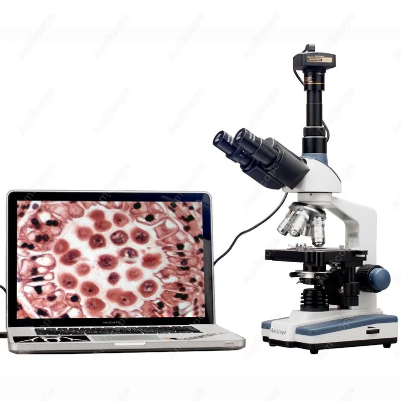 (number of dots: 1001 x 1001)
  0 – 4.0 x
  25 cm -1 (grid 75 lines/mm Echelle)
  5 mm
5 mm 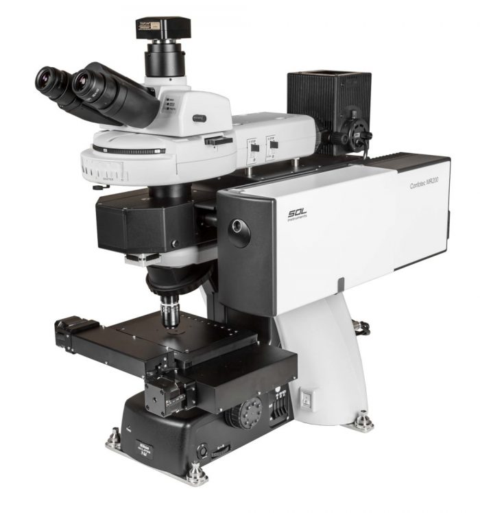 Scan area: 130 x 130 µm.