Pcb using 3d printer
DIY Homemade PCB - Etching PCBs with 3D Printers
Articles
AdminLast Updated: May 5, 2022
0 1,715 3 minutes read
Table of Contents
- 1 Overview
- 2 Materials needed:
- 3 Etching PCB with 3D Printer
- 3.1 1. Design the PCB in a software
- 3.2 2. Attach a permanent pen and plain PCB board to the printer
- 3.3 3. Home printer or set the starting point
- 3.4 4. Begin printing
- 3.5 5. Place printed PCB in an etching solution
- 3.6 6. Wipe out the permanent marker
- 4 Conclusion
In this guide, we will learn how you can make PCB at home by etching PCB with 3D Printers. Have you ever thought of creating your own PCB board? Maybe you’ve got a unique design you want to print, or you just don’t want to wait for delivery.
With a decent 3D printer that supports plotting, a few chemicals, and household items, you’re well on your way to creating a custom PCB board.
The method we’ll describe in this article is the etching method.
The principle is to expose photosensitive material to an etching solution that eats away at the surface. So, you make marks with a permanent pen on a PCB board, drop it into an etching solution, and the solution etches away the board, except for those parts covered by the permanent marker.
In the end, you’ll have a product like this:
Ready? Let’s get into the step-by-step guide on how to etch your own PCBs at home.
Materials needed:
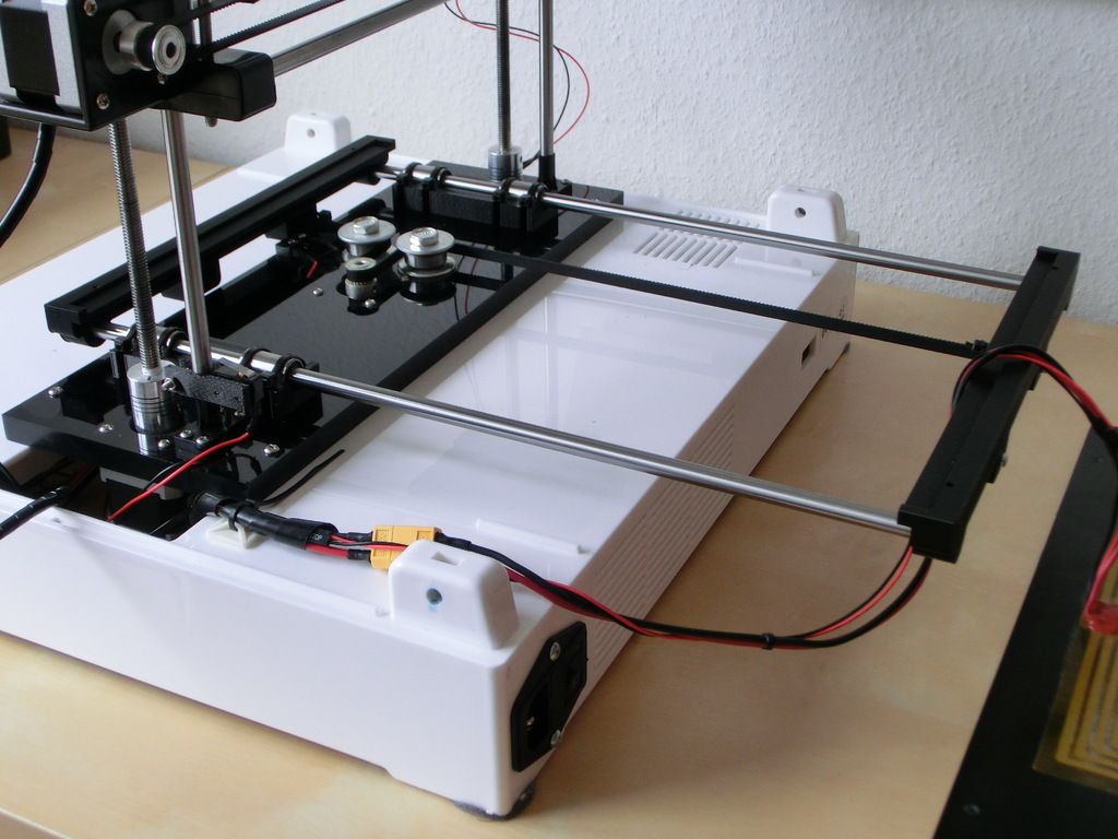
- 3D printer
- PCB board
- Etching solution
- Permanent marker or pen
- Software for designing the PCB
- Pen holder for printer
- Acetone
- Tapes
- Safety gloves and masks
Etching PCB with 3D Printer1.
 Design the PCB in a software
The first step is to create the PCB in software and export it in the appropriate format. Popular software for designing PCBs includes KiCAD, EAGLE, and EasyEDA.
The best format to export a PCB design file is the Gerber format. It allows you to create different circuit board design layers as separate image files. You can also export the design as a txt file.
3D printers most commonly read data in G-code.
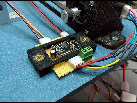
2. Attach a permanent pen and plain PCB board to the printerWhen your design is ready, attach the etch-resistant permanent pen to the printer head (sharpies can be effective). You may need to create the pen holder from scratch.
Note, that your permanent pen should have the best ballpoint diameter to neatly replicate your PCB design. A good range is 0.2mm to 0.3mm.
Next, attach the empty PCB board to the platform. This is where you use tape to hold down the board at several edges. It should be tight enough to prevent any movements.
The next step is to set a starting point for the printer and set it to act as a plotter. In the machine settings, set the temperature to 0, and the nozzle point to 1mm.
Then start the start and end codes. Set the printer to lift the pen off the board once printing is over.
I recommend homing your printer, turning it off, and rebooting it. If not, the printer will begin homing when you press “print” and therefore offset the results.
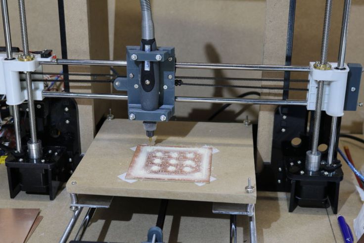
4. Begin printingWhen everything is set to run, press print. The machine will begin to plot the design on the board with the permanent marker. Depending on the complexity of the design, this process takes anywhere from 20 minutes to several hours.
If you can manage it, sit by and watch for any errors in the printing, or errors in design. You can stop the process at any time and wipe out the already made marks with an acetone solution.
5. Place printed PCB in an etching solutionWhen printing is done, and you’re satisfied with the results, place the printed board in an etching solution. The common ones are Ferric Chloride, Sodium Persulphate, and Ammonium Persulphate.
Put on safety gloves and masks. Etching solutions are extremely toxic to the skin and they may have strong smells.
The container should be wide and deep enough to comfortably contain the board, and the solution should be enough to cover its surface.
For the best results, agitate the container every few minutes. To speed up the process, you can apply temperature. Without any temperature, leave the board in the etching solution for at least half an hour.
6. Wipe out the permanent markerAfter etching, bring out the board. Dry off the solution. Then, use acetone and a microfiber towel to wipe out the pen marks.
What you’ll have is a beautifully etched PCB board, with the areas covered by the marker completely untouched.
The result is affected by how well you follow the steps and your level of experience. So be patient, as you gain more experience, the result is neater.
Conclusion
Our method only works with a printer that can also work as a plotter. Some printers make it super easy for you. SLA resin 3D printers remove any need for an etching solution.
We wish you the best of luck as you create your homemade PCB boards.
Related Articles
Make your own PCBs with a 3D printer
More PCBs, less hassle
Listen, anyone can make a PCB at home, it’s easy. PCBs (printed circuit boards) are those flat things with all the components that are inside all electronic devices, you’ve seen them. All you need is a laser printer, some glossy magazine pages, print your circuit onto the page, use a clothes iron to transfer the toner onto your copper clad, if that doesn’t work use some water and some lacquer or something, I don’t know, I stopped reading at that point because the last time I saw a laser printer, a magazine and a clothes iron was in the nineties.
Until recently, the only ways I knew to make PCBs was to practice the dark art above, to pay $10 and wait three weeks to get professional-looking PCBs from China, or to pay $60 and wait three days to get professional-looking PCBs from Europe. It was “cheap, fast, actually doable by a human person, choose two”.
That always bugged me, it shouldn’t be like that, I have always been of the opinion that there shouldn’t be things you can’t make when you have a 3D printer, but PCBs have consistently eluded me. I yearned for them, I wanted to be able to make them at home, but it seemed impossible.
One day, everything changed.
That one day when everything changed
One day, I thought it would be fun to mount a pen onto my 3D printer and got it to draw stuff (penises) on paper. If you don’t know how a 3D printer works, now would be a good time to skim my 3D printer primer, but in summary a 3D printer cuts an object into 2D slices and prints them on top of each other.
If I could take just one of these slices and tell the printer to print higher, then the nozzle wouldn’t be touching the bed, I could mount the pen lower and put a piece of paper under it, and it would draw on the paper. Getting the printing software (called a slicer) to create a 3-dimensional shape out of a photo was easy, as you can just import a drawing and it will automatically convert it to a solid.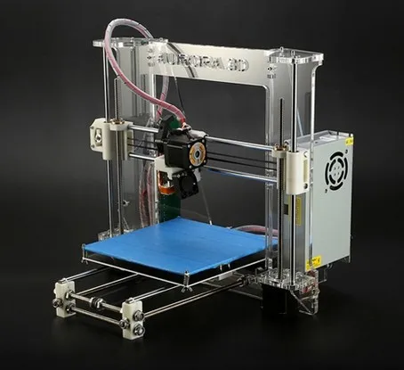
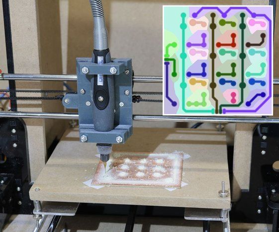
I rubber-banded a Sharpie onto a holder I quickly designed, and, a few lines of code later, my printer produced this gem (excuse quality of potato):
Your browser does not support the video tag.
My 3D printer drawing my logo onto a piece of paper.
I felt so proud of the completely useless thing I had created, I immediately ran to share it everywhere. A friend saw it on Twitter and replied that this was a good way to make PCBs.
I was immediately intrigued.
Making PCBs with markers
Apparently, all that black magic about printing and transferring and magazines and lacquer above is just a way to keep the etching acid from dissolving the copper. You see, when you’re etching a PCB, you’re basically getting acid to dissolve the copper on your copper clad (the blank PCB). Except, you’re putting something (toner) over the copper on the parts you want to keep, so the acid can’t get to it, which leaves you with copper traces.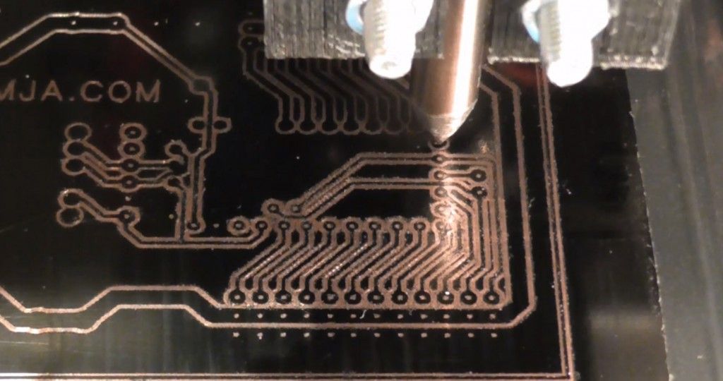
It turns out you don’t really need to do all that stuff with the toner and printer, since you can cover the copper much more easily just by drawing over it with a permanent, waterproof marker (I used an Edding 140 S 0.3mm). I had inadvertently created a plotter, which can be used for painting a circuit onto a PCB.
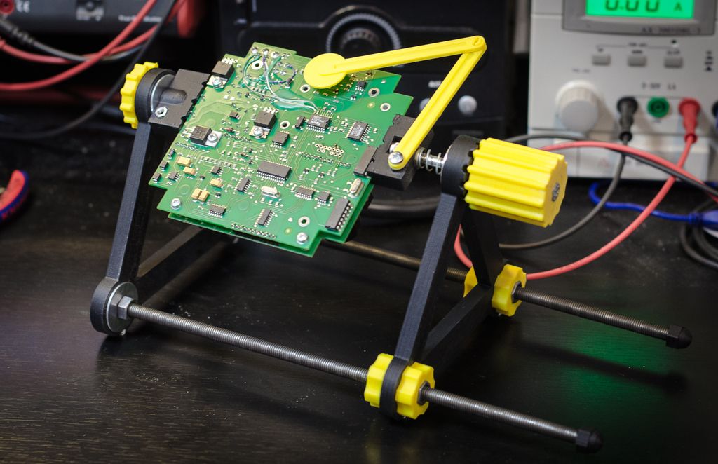
This is a signal inverter for SmartPort telemetry.
I rushed to dig out the files for one of my old, small PCBs, which you can see on the right, and ran it through my improved drawing process. I had the printer draw it on paper, just to see what it would end up looking like, and the results were pretty encouraging.
The paper somewhat absorbed the ink, as paper is wont to do, so there was some seepage, but overall the results looked like they should definitely work on copper. This is that first attempt:
That first attempt.
This looked very promising.
The improved drawing process
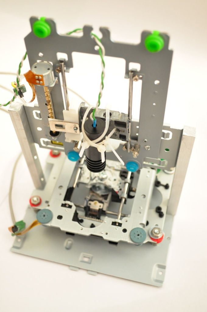
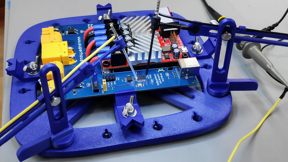
The copper clad, placed on the printer.
The original process (where I exported stuff to an image and then converted the image to a 3D model with the slicer) worked well enough, but it was meant for working with 3D models, not circuits. As such, it could sometimes lose accuracy, which doesn’t really matter if you’re printing a figurine, but does matter if it means your circuit is no longer working.
Fortunately, there is an excellent open source project called pcb2gcode, which converts Gerber files (Gerber files are basically files that describe your PCB so the fabrication factory can make it) to Gcode for various CAD tools to execute it. The Gcode that pcb2gcode outputs wasn’t compatible with my Marlin-style printer, so I adapted my script from above to turn the output to something my printer can run.
My script does various things:
- It removes commands that are incompatible with or unsafe to run on my printer (e.g. drilling commands, as it has no drill, temperature and extrusion commands, as I don’t want it to heat up or extrude, etc).
- It rewrites comments so that they are compatible with my printer (pcb2gcode comments use parentheses, my printer uses semicolons).
- It makes sure all movements are within some specified coordinates, so the print head can’t go too low or too high by mistake.
- It allows me to offset all drawing commands by some distance, so I can print exactly where I want to.
Unfortunately, as you can see on the photo of the paper drawing above, pcb2gcode has a bug where traces that are too narrow disappear, but the author is actively working on it and I worked around it in the mean time just by setting a lower marker tip diameter.
Once everything was done on the programming side, and with lots of help from my friend Andrew, it was time to actually try and draw on copper. Here’s a video of the attempt:
Your browser does not support the video tag.
Drawing a PCB on copper clad.
The drawn and cut design.
As the copper isn’t porous, the drawing looks much better than on paper. The traces are very accurately drawn, though the tolerances are a bit too tight for my liking. One trace at the top, especially, is way too close to the pad, though they aren’t actually touching. I’d have to see whether they would be bridged after etching, though.
You also might notice a small hole in the very first pad, that’s because the ink hadn’t started running yet. It was easy to fix by just painting it in with the marker at the end.
The only thing left to do is take some of that copper layer away so we’re left with our traces.
Etching
Carefully weighing and diluting the sodium persulfate.
Surprisingly (and as my friend Josh rubbed in with what I imagine to be considerable glee), the actual etching part wasn’t as easy as I thought. It wasn’t hard, but it also didn’t consist of just throwing the PCB in acid and waiting.
I’m still in a trial-and-error phase, as I’ve only etched two PCBs, but it seems like 100 grams of water with the appropriate amount of sodium persulfate dissolved in it is only good enough to etch a tiny PCB. If that’s true, it will take a lot of acid to etch a larger one, but I’ll have to experiment and see what happens.
UPDATE: Some commenters on HN pointed out that the reason this took so long was that I didn’t have a copper plane. I decided against that initially because I didn’t want the marker to have to basically paint the entire PCB, but after having etched, it’s definitely worth it. A plane makes it so that a lot of the copper is left on the PCB, and only the outlines of the traces are etched, which is all you need anyway. This way you aren’t wasting your etchant trying to etch a lot of copper, it takes less time, and your PCB ends up better etched.
The other thing I’ve learned is that you shouldn’t heat the water above 50ish C, otherwise it starts to vapor and that can’t be good for anything.
Also, the first time I etched a PCB I kind of just left it in the acid, but it turns out the copper dissolves much faster if you’re agitating or stirring the mixture. I started looking into designs for building an agitator for subsequent tries, but then realized that you don’t need one if you have a 3D printer, and wrote this Gcode file instead:
Your browser does not support the video tag.
You seem agitated.
It even heats the bed to 40 C so your etchant is kept warm! Is there anything 3D printers can’t do? Doesn’t look like it!
Etchant health concerns
I have no idea what the health concerns for these chemicals are. I’ve kind of just tried to avoid getting too close to the vat, even going as far as to put the lid on the tupperware container I was using, but I don’t know whether that delays or somehow impedes the etching process.
It’s been hard to find info about all these chemicals, so if you know anything, please leave a comment below or send me an email, especially if you know of a better/more convenient/safer etchant. I will update the article with any info as it comes, for the edification of anyone who reads this.
UPDATES:
throwanem on HN says that sodium persulfate isn’t too bad, the biggest problem is fumes which can be kept to a minimum at low temperatures. Higher temperatures accelerate the etch, but the fumes shouldn’t be inhaled. It’s also a fire risk, and should be kept cool and dry.
As always, any etchant should be safely disposed of and not poured down the drain.
The etching continues
The PCB is bubbling.
Etching was otherwise uneventful, the PCB started bubbling at some point and then it started flaking, and the etchant turned slightly blue, which I assumed meant it was working. Agitating it a bit made it flake more, which seemed like a very good sign, so I just kept doing it and it kept working. I then left the mixture to its own devices because I was getting bored, until I noticed it was finally done.
Eventually I was left with a slightly over-etched but otherwise extremely respectable PCB. I don’t know why the over-etching happened, I imagine it was because I left it in the etchant for half an hour. Maybe I need to use more etchant for it to go faster and not have time to over-etch, I hear it should ideally take from three to ten minutes.
Regardless, with no small amount of pride, here’s my first ever home-etched PCB!:
The final product. I'm so happy.
It both looks good and works well! I tested everything with the multimeter and everything that should be connected is connected, and nothing that should be disconnected isn’t disconnected.
All in all, I would call this an unconditional success!
This was all a ploy
Of course it was a ploy! What did you think, that I spent all this time, effort and tax payer dollars to create a signal inverter for an RC airplane? Don’t be naive.
My ultimate goal was far more nefarious, and with Andrew’s help my life-long dream is now a reality. I present to you this:
The Richard Rear PCB, the pinnacle of human innovation.
Yes, that is a dickbutt PCB with a red LED on the dick on its butt.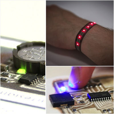
If you don’t know whether to laugh or cry, you are exactly right, because that’s precisely what I was going for.
Epilogue
I am extremely excited about this process, as it finally allows me to easily make PCBs at home, quickly, conveniently, cheaply and at rather high tolerances, for what it is. I have been looking for something like this for ages, and I really think it could spark a minor revolution with hardware enthusiasts. It’s definitely much faster, better, more fun and more convenient than soldering protoboards, which I hate hate hate.
If you want to do this at home, all my code, Gcode files and process documentation are in this repository:
https://gitlab.com/stavros/pcb-plotting
Feel free to open an issue if something isn’t working properly, or a PR if you want to improve something. I’d appreciate your help.
Also, as always, please Tweet or toot at me, or email me directly.
Printed circuit boards using a photopolymer 3D printer / Sudo Null IT News And in the last year or two, thanks to a strong reduction in cost, their photopolymer subspecies is also flourishing.
 Now such a printer is already available to almost everyone, and the number of their models on the market is multiplying every month.
 Even when I just learned about the appearance of a new type of photopolymer printers a few years ago - in which the image of the layer for illumination is formed by an LCD, the thought flashed through me already then: "Hmm, what if we substitute a photoresist on a textolite?". But then it was a purely theoretical question - the prices for them were considerable, and the resolution and display area left much to be desired. However, today these printers can already boast of a decent resolution - from 30 microns per pixel, and a completely normal display area.
And as it turned out, with the help of an inexpensive modern photopolymer printer, it is quite possible to make boards with tracks / gaps from 0.15 mm.
I apologize in advance for such a voluminous graphomaniac, I myself did not expect that the note would get so fat...
I foresee the question "But why? In China, they will make normal boards with a mask and silk-screen printing for a penny!" I answer: now, most likely, there will be several iterations of finishing the board to a satisfactory state.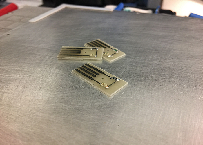 I made a board - tested it - made corrections. And so several times. Waiting every time for 2-3 weeks from China is not an option :) But when the final design of the board is determined - then, of course, normal production in China or on Rezonit.
Now let's get down to business.
Who does not know - here is a brief principle of operation of such a printer The main part of such a printer is an LCD display. Below this display is a 405 nm UV source. Above the display is a bath of photopolymer, which has a thin transparent FEP film as a bottom. A platform is lowered into the bath, on which the model is “grown”. At the beginning of printing, the platform lowers to the height of one layer from the film, the image of the first layer is displayed on the display, and UV illumination is turned on for a specified time. Illumination, getting through the "open" pixels of the display and the film onto the photopolymer, hardens it, so a hardened layer is obtained. The first layer sticks to the platform.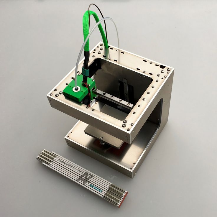 Then the illumination is turned off, the platform rises to the height of the next layer, the image of this layer is displayed on the display, and the illumination is turned on. The second layer is cured by welding with the previous layer. And this is repeated over and over until the entire model is printed.
The idea to try to make a printed circuit board using such a printer came to me again about three years ago, when I bought myself an Anycubic Photon S printer. , then I just forgot about this idea, because and there was no need to make boards. But the other day, the need arose for the manufacture of several small boards, and with a high probability that as tests are made, changes will be made to these boards and it will be necessary to go through several iterations of "manufactured-checked-changed" in a short time. And the idea resurfaced.
To be honest, I thought that by now the Internet would be filled with the results of such experiments, the idea lies on the surface :) But to my surprise I found that the Internet is almost completely silent on this issue.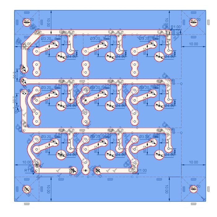 There are separate notes, but there is no integrity and completeness in them. That's why I decided to publish this post - maybe it will help someone go all the way faster than me, and with less rakes :)
Well, the most important thing is that you don't need film and you don't have to struggle with increasing the contrast of the template. You also do not need a separate UV source with a place for its installation. And, of course, it is stylish, fashionable, youthful.
There are also disadvantages - the resolution of most modern 3D printers still does not cause much enthusiasm yet - the pixel size of all fluctuates around 0.05 mm. But this is already enough for confident manufacturing of boards with tracks from 0.2 mm and rather high chances of success with tracks from 0.15 mm. Due to the raster nature of such a template output, the position and size of elements on it can vary + -1 pixel, so I think it’s not even worth counting on tracks of 0.1 mm or less.
Let's go in order.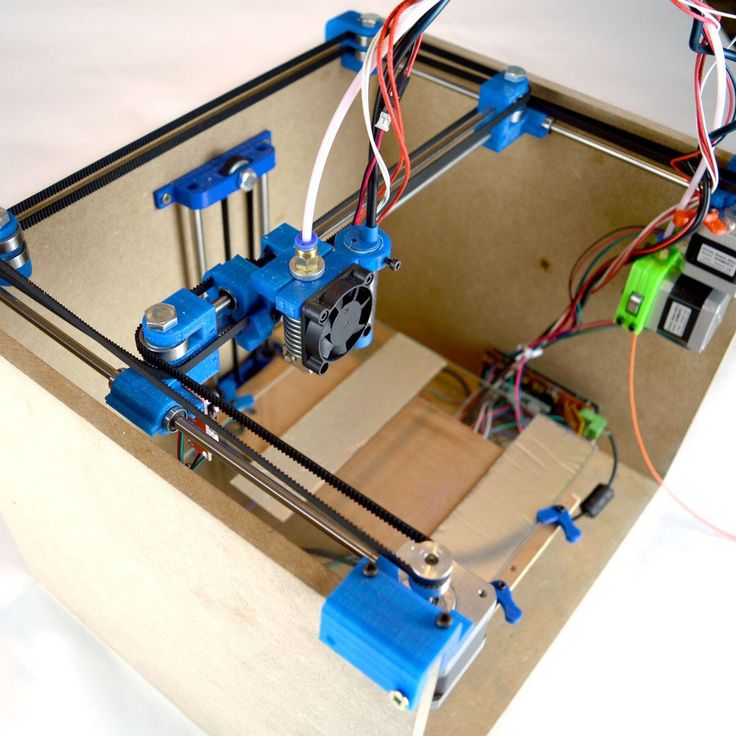
Task
It is necessary to make a printed circuit board at home using photoresist. Instead of templates and illumination lamps, use a photopolymer 3D printer that will serve both at the same time.
Let's divide the problem into separate steps-solutions for each moment.
-
Board development
-
Outputting layers in a printer-friendly format
-
Preparation of textolite with photoresist
-
Printer flare
-
Photoresist development, board etching
1. PCB development
Well, there are no questions. Whoever prefers to work in what program - in that one makes boards. The main thing is that the program should be able to display the result in some commonly used form. The easiest way I've come up with is outputting board layers to gerber files that can be fed to an online service. But you can also output to PDF or images.
2. Converting the CAD output to a printer friendly
This is where the trouble begins.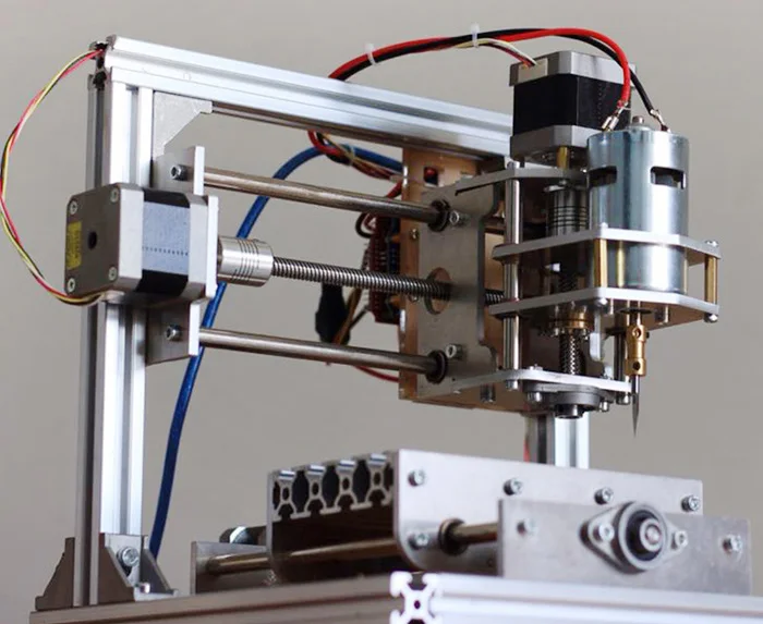 If almost all CADs can output to generally accepted formats - gerberas, DXF, printing to PDF, then 3D printer manufacturers so far categorically refuse to accept any file standard. Everyone is perverted as they can. The situation is largely saved by the fact that many manufacturers use motherboards from one Chinese company, Chitu Systems, in their printers. Thanks to this, many printers on such boards are able to understand one of the basic formats developed by the same company. And even often, if a file has some unique extension, then in fact it has the same basic format, just with a different extension. But it may differ in some details.
In any case, there is a free UVtools utility known among photopolymerists that can open files in one format and convert them to another format. It understands almost all formats on the market :)
I have tried two ways of preparing files with layers for the printer and I will describe both.
2.1 Gerber output and conversion to .
 photon
 The .photon file format is understood by the old Anycubic printers - Photon and Photon S. This is exactly the case when the printer manufacturer took the format from Chitu and changed its extension. In the original, this is the Chituvian .cbddlp format, so you can safely change the extensions of these file types among themselves and the printers will devour them like native ones.
Since I have a printer that understands this format, this method suited me perfectly. The limitations of this method are that the printer must understand .photon or .cbddlp files and have a standard display for most non-monochrome printers with a resolution of 2560x1440 and a diagonal of 5.5". manuals on how to do this for any CAD that can, in principle, mirror layers or not - it makes no difference, they can be mirrored in the utility during the conversion process.0003
Now open the online utility for converting gerber files - https://pcbprint.online/ and load the gerberas into it. By the way, this is a utility from a Russian developer who lives here.
It is easy to understand, although it does not contain any information or help. But here is a short guide:
For a single-sided boardUpload your gerbera in the main window with the "Upload file" button:
We made sure that everything is fine and the image meets expectations, if necessary, make a negative or mirror the image with the buttons in the top center, and press the button " Render layout":
Now press "Lauout" at the top right and get into another screen:
Here you first need to go to the settings (gear button at the top right) and there select the format of the output file "photon":
The time in "Exposition" can be left at default and change it to the desired one directly in the printer. But you can immediately put the right one if its value is already known :)
Close the settings and return to the previous screen. Here the output image is on a black space showing the working field of the printer.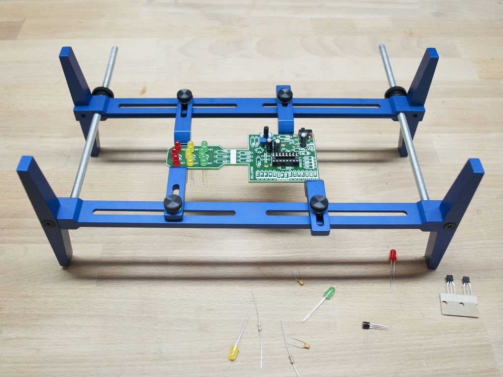 The image can be moved, aligned. When everything suits, we first press "Render", and when the "Download result" button next to it becomes active, we also press it. And save the proposed .photon file to a convenient location on your computer :)
For double-sided boards, things are a little more complicated due to the need to match them. Therefore, it is necessary to know very exactly the position of the image displayed on the printer's display in order to place the board on the display very accurately in accordance with it.
I had several options for solving this issue, but in the end I decided on the simplest of them, which did not require any mechanical conductors. To do this, I still in CAD in a separate layer (it is possible in the border layer or in any other "unnecessary" layer) I draw a frame around the board with a line of 0.15 mm and indented from the edges of the board by 0.25 mm. As a result, I get three gerberas - the top layer, the bottom layer and a separate empty frame.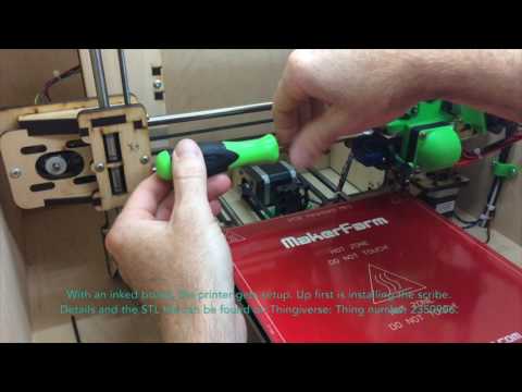
I upload all three gerberas to the above site and then in a few steps I get three files for the printer.
Double-sided board in pcbprint.online/So, all three gerberas have been loaded. All of them are mixed together, but it's not scary:
Now hide the top and bottom layers, leaving only the frame (by clicking on the eyes in the names of the gerberas).
Click "Render layout" and go to the "Layout" screen with the button in the upper right corner. We see an empty frame, drag it to the desired position on the black field of the display, click "Render" and "Download". The first file for the printer is ready.
Switch back to the gerber screen with the "PCB comose" button. Redisplay the first layer (the frame layer still remains visible), mirror if necessary, and click "Render layout" again. Again we go to the output screen and now there are two pictures hanging on the display field - a separate frame and the first layer with a frame. The frame remained in the same place where we pulled it last time. And now our task is to exactly combine the frame of the first layer and the empty frame:
Click "Increase" and combine in one of the corners. In this case, in no case should you move the empty frame that we set in the last step!
Combined, click "Render" and "Download", and we have a second file for the printer. Before returning to the gerbera screen, we delete the render layer with the frame, we should again have an empty frame. And now we return to the gerberas, hide the first layer and display the second one, look at the need to mirror, click "Render layout" and go to this screen again. In the same way, we combine the layer frame with an empty frame (which cannot be moved!), then "Render" and "Download".
Everything, all three necessary files for the printer are ready.
All this hemorrhoids allows you to generate for the printer files of an empty frame and layers with a frame in the same place on the printer display with high accuracy. The empty frame serves to aim the board, more on that below.
If necessary, the resulting .photon files can be converted to the desired format using UVtools :)
2.2 Output layers to PDF or images
The second method is perhaps more confusing, but its great advantage is versatility, it is suitable for any printers, whose formats are supported by UVtools. I will describe it only in general terms, because. There are quite a lot of tools and specific ways to implement it, and everyone can choose them according to their preferences.
So, the goal of the first step is to get a picture with a size equal to the resolution of the printer's display, preferably in a lossless compression format. In this case, the image of the layer in the picture must correspond to the real size in the scale of the display.
If CAD allows you to output directly to the picture - great, output to it. If the resolution of the output image is configurable - specify the resolution of the printer display. It is elementary to calculate it - we divide the number of pixels across the width of the display by the width of the working area in mm and multiply the result by 25. 4, we get the resolution in pixels per inch. If the resolution is not set, then set the image size as large as possible so that there are at least 15-20 pixels per 1 mm of the board.
If output to image in CAD is not available, then output to PDF. This PDF will need to be opened in another program and converted to an image. Photoshop, Corel, maybe other programs can do this... The requirements for image resolution are the same. For example, in Photoshop, when importing a PDF, you can immediately specify with what resolution to convert to an image. For example, for common displays with a resolution of 2560x1440 and a diagonal of 5.5 "the resolution is approximately 537.566 PPI (pixel size - 0.04725 mm).
The resulting image will need to be changed in some image editor, bringing its size to the resolution of the printer's display. In this case, the layer image must be scaled to the real one (taking into account the pixel size of the printer display) or saved without scaling if the PPI of the display was specified when importing the image.
UPD: in the comments @0x3f00 gave a link to his converter of PNG images to files for the .photon printer - https://github.com/0x3f00/PhotonCpp/releases/tag/v1.0.0 . There is also an instruction for using it just for the purpose of manufacturing boards - https://github.com/borelg/PhotonPCB.
2.3 There is another way, but it is very resource-intensive
You can output layers to PDF, then open this PDF in Corel, convert it, save it in DXF, extract a three-dimensional object from this DXF, which you can push into the printer's slicer.
Necessary transformations in the vector editor:
-
Connect all curves.
-
Convert outlines to objects.
-
Merge intersecting objects.
You can extract a three-dimensional object from DXF, for example, SolidWorks. Fusion360 also seems to be able to. Who else is capable of this - I honestly don't know, but in theory any CAD that can import DXF as a sketch.
Thus, for example, I made a model for determining the exposure time of the photoresist.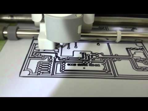
3. Preparation of textolite with photoresist
The Internet is simply littered with articles on this topic, but for the sake of integrity and for the sake of some specific points, I will also describe such well-known stages as the preparation and etching of textolite.
My first experience with such a fabrication was a couple of days ago with a domestic photoresist PF-VShch. Taking into account the last yesterday's experience, I categorically advise not to waste time on this photoresist, but immediately take a decent one - Ordyl Alpha 350(330) :) They say that Kolon is also decent, but I have not tried it. With Ordyl photoresist, the results are much more stable and accurate, it is easier to develop and adheres much better to the foil. And he can forgive those mistakes that will be critical for the PF-VSC. And what is important - it is sold in a bunch of places quite inexpensively.
3.1 Preparing the textolite
To begin with, the textolite should be smooth, very preferably with a smooth foil without scratches or dents. Otherwise, the chances of success are reduced.
If a double-sided board is being made, then you need to immediately cut the board out of the PCB exactly to size. If there is any CNC router, then you can drill all the holes and cut along the contour in one installation, as I do. If not, then it is better to leave the drilling for later, when the board is etched.
After this, the textolite blank must be very carefully cleaned and degreased. This can be done with a kitchen abrasive sponge (but not used for washing dishes on which fats have already accumulated) and a scouring powder like Pemolux. Very carefully, slowly three every square millimeter of foil, without touching it with your fingers. In general, I categorically do not advise touching the foil with your fingers after the start of cleaning, there should not be the slightest even the faintest greasy spot on it. After cleaning, rinse thoroughly in running water, shake off excess water and allow to dry. I do not advise blotting or wiping with anything, because.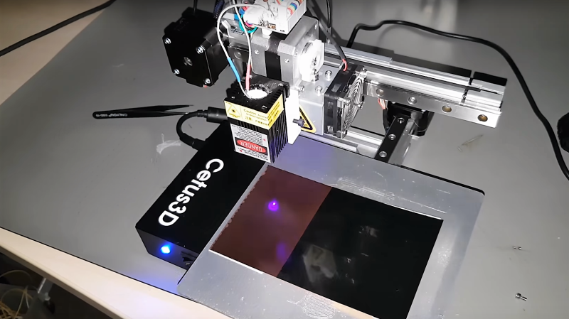 grease can be applied, even from a new napkin.
3.2 Application of photoresist
Also a fairly common topic on the Internet, so I'll go over it briefly.
Photoresist usually comes in sheets or rolls. It consists of three layers - two protective films and the photoresist itself between them. A piece is cut off from the photoresist according to the size of the board + 5 mm in length and width, then a matte (polyethylene) protective film is removed from it.
the second, glossy (lavsan) must remain on it until the etching stage.
The easiest way to remove the film is with a piece of tape. It is glued with its edge to the corner of the photoresist and then folded back, pulling the protective film along with it.
After removing the matt film, the photoresist is applied to the edge of the board and smoothed along this edge with a finger. The rest of the photoresist is supported by weight, without tension, but in such a way that as little as possible of its area lies on the foil.
Please note that if the Ordyl photoresist falls on a well-prepared textolite, then it can firmly stick to it, and without bubbles it can no longer be rolled. You have to scrape it off and do it all over again. And PF-VShch can fall as much as you like - it definitely won't stick :)
Now the knurling itself. If you have a laminator, in which the textolite will crawl through the thickness, then it's just wonderful. We make an envelope-type strip of paper folded in half, put a textolite with a sticky edge of the photoresist in it, and serve this sandwich into a laminator heated to 100-110 degrees. At the same time, we continue to hold the photoresist so that it comes into contact with the textolite foil only directly at the inlet of the laminator.
That's all for Ordyl, for PF-VShch it will be harmless to roll a couple more times.
If there is no laminator, then smooth the photoresist to the textolite with your finger from edge to edge, gradually lowering it onto the textolite.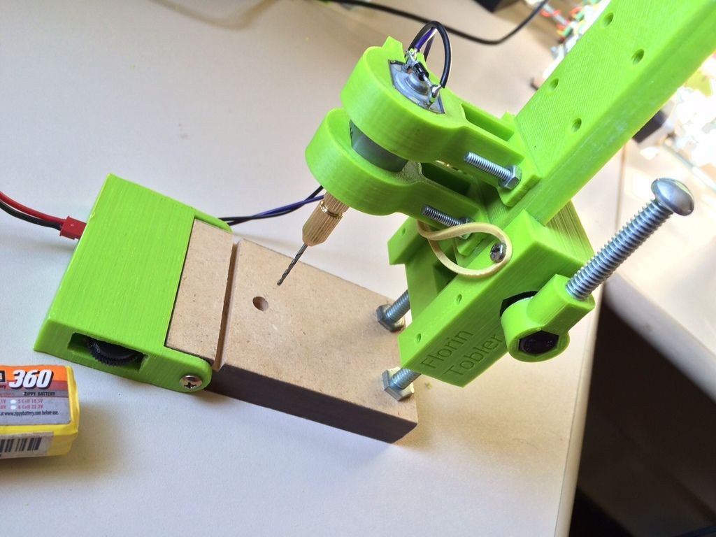 The main thing is not to catch the bubbles. After all the photoresist lay on the foil, we take a hair dryer and heat the textolite to 70 degrees, after which we iron the entire photoresist once again.
After knurling, let the textolite with photoresist lie down for 15-20 minutes, or at least until they cool down to room temperature - according to the recommendation of the photoresist manufacturer.
And now everything is ready to highlight the layer pattern :)
4. Printer highlights
I want to warn you right away: looking directly into the glowing display of a photopolymer printer may not be very good for the eyes. Although not true UV (405 nm), the brightness is quite noticeable and can be harmful to the eyes. Therefore, I recommend using colored or tinted goggles. I think even sunscreen will do.
First, you need to remove the bath and platform from the printer, they are completely unnecessary for this business and even interfere. This completes the preparation of the printer :)
Lighting also has different options. If you have a one-sided board and the blank is larger than the size required for the board, then everything is simple - throw the file obtained at the preparation stage into the printer and, knowing the approximate place for displaying the image on the display, put a textolite with photoresist in this place. Then start printing the file and wait until it is completed. Everything, the photoresist is exposed, it is possible to develop.
If the workpiece is equal in size to the board being made and the error with the position of the workpiece on the display is unacceptable, then in this case it is necessary to remove the frame during preparation, as is the case for a double-sided board. Illumination also occurs using a frame, similar to a double-sided board, only without the second side and the second layer.
So, the illumination of the double-sided board. We throw all three files into the printer - with a frame, with the first layer and with the second layer. We put the workpiece next to the printer in quick accessibility.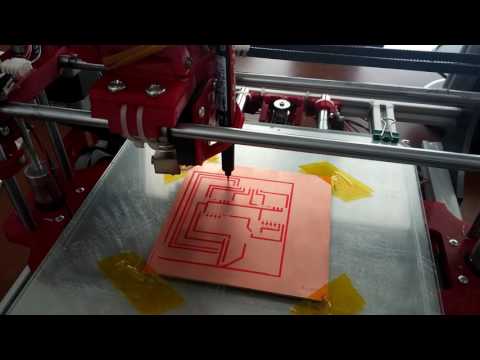 If it is already pre-drilled, it will be useful to make sure that it lies in the correct position so that you can quickly take it and immediately put it on the display. To do this, we run a file with a layer planned for exposure, and compare the layer pattern on the display and the orientation of the board next to the printer.
Printing a file with one frame. As soon as the frame lights up on the printer display, we take the workpiece and put it approximately inside the frame. While the frame is being illuminated, we align the workpiece so that it is exactly in the frame, with the same indentation of the frame from the edges of the workpiece on all sides.
In the photo, I gave an example with a ready-made board, because I did not take pictures during the manufacturing process. Well, reflections interfere quite strongly, alas... But I think it's understandable :)
That's it, the position of the workpiece is verified, printing of the frame file can be interrupted or wait for it to finish. Without moving the workpiece, run the file with the first layer and wait for it to finish. We illuminate the second layer (the second side) in the same way - we launch the frame, place and align the workpiece, without moving it, we launch the second layer. Before this, just in case, you can make sure that the workpiece will lie in the correct orientation, as before the first layer.
If the workpiece is not completely flat and does not fit the entire area of the display, then you can press it down from above with some heavy flat piece of iron. You just need to make sure that this piece of iron does not interfere with the platform lever, which will go down with the start of printing - the printer thinks that this is a normal photopolymer print and you need to lower the platform to the bottom of the bath :)
Illumination time can be different from printer to printer . It depends on the power of the emitter, and on the optical illumination system, and on what type of display is worth - monochrome or RGB. Here already it is necessary to select each individually. For orientation, I can say that I got the best result with the Ordyl photoresist at an exposure time of about 90-110 seconds. With photoresist PF-VShch - about 10-13 minutes. Printer with paraled, illumination power slightly less than 50 watts.
After exposure, the workpiece should be allowed to rest for 15 minutes - this is according to the recommendation of the photoresist manufacturer. Ordyl changes the color of the highlights quite noticeably, so it's pretty easy to control the highlights. Unfortunately, the photo did not convey it well, it can be seen better with the eyes.
5. Development, etching
Everything here is according to the recommendation of the photoresist manufacturer and according to the classics of the Internet.
All necessary chemicals were purchased inexpensively from Auchan. Even hydrogen peroxide 6% - this was a surprise for me, I had never seen it in hypermarkets before, and even in liter bottles.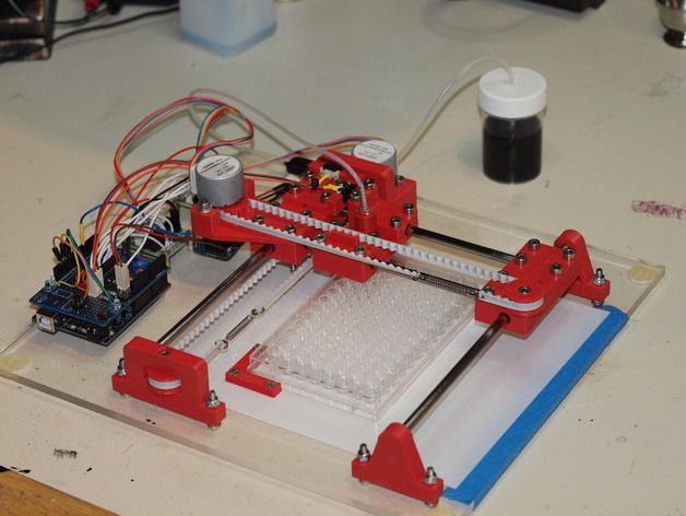
For one session you need:
-
Soda ash - 1.5 grams
-
Hydrogen peroxide - 150 ml for 3% (or 75 ml for 6% + 75 ml of water)
- citric acid
-
Salt - 7.5 grams
-
Alkali (caustic soda, sodium hydroxide) 5-7% - 100 ml
With the cheapness and ease of buying all the components around the corner, I am in favor of preparing a new solution for each board. Although the etching solution, as they say, is not stored anyway. A solution of soda ash noticeably "poorer" in the process of development. Unless caustic soda can be reused, but is it worth it to keep another bottle ...
Both Ordyl and PF-VSH appear in a weak solution of soda ash. For PF-VShch - 1-2%, for Ordyl - 0.8-1.2%. For Ordyl, we take 150 ml of water and dilute 1.5 grams of soda in it. The solution can be heated up to 30 degrees, this will speed up the development, but it is important not to overdo it, otherwise the illuminated areas may begin to be damaged.
Ordyl appears rather quickly. Already after 10-15 seconds, the illuminated pattern begins to become more and more contrasty, the unexposed areas gradually dissolve, become thinner and become paler.
To speed up the process, it is recommended to shake the bath so that the reaction products are washed off the surface of the workpiece. For this I adapted my old 3D printer, its table and shook and heated the bath with the solution during development and etching :) Two minutes passed before there were at least some signs that development had begun. In addition, if Ordyl does dissolve, then PF-VShch first swelled like gelatin and discolored, and only then began to slowly dissolve.
At the end of development, you can go over the boards with a hard paintbrush (or soft toothbrush) several times in different directions to help flush out any remaining photoresist from tight spots. Ordyl holds on tight, this procedure should not disrupt it, but with PF-VShch you need to be very gentle, even without a brush it strives to exfoliate on thin paths.
After etching, the workpiece must be rinsed in cold water so that the soda residues do not continue to attack the photoresist and so as not to clog the etching solution with them.
The result should be something like this, maybe even better :)
More detailsScale of the grid square - 0.2 mm:
The scale is the same. Here you can see the raster component of the illumination, the pixels stick out:
Etching was also done according to the traditional recipe, popular on the net:
It is better to heat the solution to 40-50 degrees, then the etching goes much faster. This is my first experience with this solution. I used to poison with ammonium perchlorate, and even earlier - with classic ferric chloride. To be honest, I can't really express how I feel about this solution. On the one hand, it poisons rather quickly, is transparent, does not get dirty, and is relatively safe. On the other hand, it seemed to me that it was easing quite a lot ... But maybe it just seemed, I haven’t been making boards for 10 years and I forgot how it all worked when the trees were big :)
After etching, the exposed photoresist must be removed from the workpiece, and this is done in caustic soda.
 On my bottle of cleaner it says "at least 5% but not more than 15%" and it takes 5-8% to remove the photoresist. I diluted the product 1:1 with water and this solution did the job perfectly. The photoresist does not dissolve in it, it simply peels off the foil after 2-3 minutes and begins to float in tatters in the solution.
 After that, the board is thoroughly rinsed under the tap and... The board is ready!
Summary of my experience
Overall I am satisfied. I did not expect to get tracks / gaps of 0.1 mm and I did not get them. Here, the capabilities of the printer are severely limited (pixel size), and in general, good experience is needed for such results. But I was hoping to get at least 0.2 mm, and if I'm lucky, then 0.15 mm - and I got it. 0.2 mm confidently, 0.15 mm - well, so-so... If you try, you can achieve :)
There were some flaws - it was not pickled in some areas, and imperfect alignment of layers and holes. But neither is critical. As for the non-mordant - I think that I just hurried to take it out of the developer, I was afraid after PF-VShch that thin paths would begin to peel off.
 Although in the reviews people write that it is quite difficult to re-develop this Ordyl, you need to try for this. Imperfect alignment of layers and holes is to be expected. From such a simple method of alignment, I expected an error of 0.1-0.2 mm, which I got, but it suits me.
 Thank you for reading.
And finally, a few photos of my results. Exposure time test, from 1 to 2 minutes. You can see the sites displaced relative to the holes. printerI'll tell you how you can make a board at home using Delta Design. The order of work is something like this: Delta Design -> DeltaCAM -> FlatCAM -> 3D printer with laser pointer . In my hobby, I periodically need to make prototyping boards to test and / or connect microcircuits with minimal strapping, in this case, an example will be for connecting a MAX5725 DAC.
As a final result, we need to get a gerber file for one layer of copper and, possibly, another layer for a protective solder mask, but why bother with trifles - then also prepare the silkscreen and make a stencil for the paste .
 .. but that's for another time.
 It all starts with the component library. Footprints for SMD components do not differ much from those for a multilayer board or a single-sided, more precisely, single-layer, except for different soldering modes - manual, paste, wave, or something else. For home use, manual soldering is more often used or on paste, also manual, i.e. not automated. But with DIP components, things are different, because. there is no plating in the holes, and in order for the platform to hold the component well, its size is increased. Thus, for hand soldering and single-layer boards without hole plating, it is reasonable to make a separate library of components. Yes, and the set of rules will have to be corrected in order not to make paths too thin without urgent need, because. the wider the traces and gaps, the easier it is to control the PCB manufacturing process. Further, the process of designing a printed circuit board is no different from the industrial version.
What Delta Design lacks for single layer boards is automatic SMD and/or DIP jumper placement. But even without this, it is possible to design a board, however, it is not very comfortable, if I may say so.
When the library is prepared, we start creating the board. Everything is simple here, the main thing is not to forget to immediately indicate the 3rd class of accuracy - it is quite feasible for home production.
In addition to the rules, you can also choose the format right away, if the scheme is not large, then I choose the A4 format:
Let's move on to creating a circuit and a printed circuit board layout - this is a creative process and everyone does it in their own way. Prepared the circuit and board:
On the DOCUMENTUM layer, I added graphics - text and a circle for later merging on the copper layer along with the PCB layout.
The only thing you need to pay attention to is the choice of grid for the board editor. By default, there is only a millimeter grid, but often you have to make boards with pin connectors like PLS. And then I insert such scarves into the circuit board with holes with a pitch of 2.54 mm or connect them with wires with Dupont connectors. So, in order to put the connectors at the right distance, a multiple of 2.54 mm, it would be convenient to switch the grid to this step and arrange the connectors. The grid setup for the board needs to be done in the standards once:
There's a tricky grid setup relative to the base grid:
Added grid 1.27 and 2.54. The mesh can now be toggled in the PCB editor in the lower left corner.
About once, I lied. Delta Design is frequently updated and needs to be reinstalled frequently. Therefore, if you set it up for yourself once, then you need to export the standards to a DDS file and, after the next update, import the standards before starting work with the new version of CAD.The board is designed, the only thing left is to upload Gerber files to production .
 .. But there are also a few points here, which I will dwell on in more detail. For a single-layer board, I usually combine the outline of the board, the copper layer and graphics, for example, put a logo or make inscriptions. In addition, checking the output gerber file in the viewer is also useful.
 In Delta Design, export to gerbera is called differently: “Create Production Files”
In the form, select which layers you want to display and indicate that all this should be saved in the project tree. If you need to look at the files in an external viewer, you can choose to save the files to disk.
After creating the production files, a line with the factory icon appears in the project tree:
Open this item and see all the layers that we have selected. This is a DeltaCAM Gerber file viewer and editor already built into Delta Design.
Here you can already transfer the graphics from one layer to another. Select the desired layer with graphics, select all the necessary objects and change the layer for them in the properties:
Thus, we transfer everything to the SIGNAL_TOP layer. The peculiarity of this operation is that during such an operation there is no conversion of graphics and objects in the Gerber file. They are simply transferred without changes.There remains one more necessary operation - this is the addition of holes on the apertures of DIP components for subsequent drilling at home - the hole must be smaller than the diameter of the drill, because. it is only needed to guide the drill while drilling the board. To do this, in the aperture editor, find the necessary apertures and change their hole diameter.
In this example, two apertures are needed for drilling - an oval and a rectangle, DCode 5 and 16, respectively. We make the hole diameter minimal and sufficient for etching at home. This operation also does not change the graphics of the Gerber files, as simply complements the parameters in the description of the aperture according to the Gerber standard. As a result, we immediately see the changes:
The board is now ready for production. We upload the Gerber file of the desired layer and prepare it for making a photomask, a picture for a LUT, or for laser illumination on a home CNC machine, such as a 3D printer. Uploading the edited layer to a file is done through the creation of production files, only not according to the board, but according to the CAM project:
We select one layer, because. we threw everything there and create it as a Gerber file.Further, the ways of manufacturing a printed circuit board may differ. In my example, I will illuminate the photoresist using a UV laser pointer installed on a 3D printer. There is no functionality in DeltaCAM with which you can generate a GCode for execution on a CNC machine, for this stage I use FlatCAM (http://flatcam.org). Details about connecting a laser pointer, GCode preparation described in another article.
I note that FlatCAM does not support holes in apertures, which is written on their website: http://flatcam.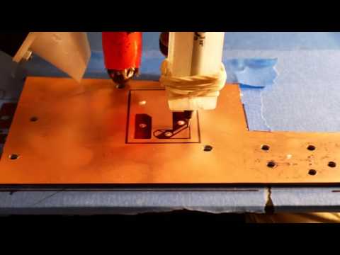
Learn more