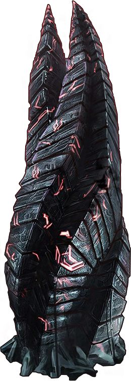
3D printed dead space marker
Dead Space Marker STL File for 3D Printing File Only
Etsy is no longer supporting older versions of your web browser in order to ensure that user data remains secure. Please update to the latest version.
Take full advantage of our site features by enabling JavaScript.
Click to zoom
Star Seller
Star Sellers have an outstanding track record for providing a great customer experience—they consistently earned 5-star reviews, shipped orders on time, and replied quickly to any messages they received.
| 2,419 sales |
5 out of 5 stars€3.80
Loading
VAT Included
Star Seller. This seller consistently earned 5-star reviews, shipped on time, and replied quickly to any messages they received.
Listed on Oct 6, 2022
177 favorites
Seller Information
Report this item to Etsy
Choose a reason…There’s a problem with my orderIt uses my intellectual property without permissionI don’t think it meets Etsy’s policiesChoose a reason…
The first thing you should do is contact the seller directly.
If you’ve already done that, your item hasn’t arrived, or it’s not as described, you can report that to Etsy by opening a case.
Report a problem with an order
We take intellectual property concerns very seriously, but many of these problems can be resolved directly by the parties involved. We suggest contacting the seller directly to respectfully share your concerns.
If you’d like to file an allegation of infringement, you’ll need to follow the process described in our Copyright and Intellectual Property Policy.
Review how we define handmade, vintage and supplies
See a list of prohibited items and materials
Read our mature content policy
The item for sale is…not handmade
not vintage (20+ years)
not craft supplies
prohibited or that use prohibited materials
not properly labeled as mature content
Please choose a reason
Tell us more about how this item violates our policies. Tell us more about how this item violates our policies.
All categories
Craft Supplies & Tools
▷ dead space marker 3d models 【 STLFinder 】
Dead Space Marker + Stand
thingiverse
this is the Dead Space marker attached to the stand, no need to worry about messing around with scaling *Under no circumstances do you have the right to take this file and use it for profit!*
DEAD SPACE MARKER And base
thingiverse
Dead space marker, Base
Dead Space Marker LED-Base
thingiverse
This is a plate for the dead space marker base from bluekingdom, for when you want to add custom LEDs to the base. ...Fits 8 LEDs, which in my case, where then connected to an ATTiny to create a circular led movement.
dead space marker necklace
myminifactory
A necklace with the symbol of the marker. ... let it guide you through the halls of the ishimura.
dead space marker necklace
thingiverse
A necklace with the symbol of the marker. ... let it guide you through the halls of the ishimura.
dead space marker lamp base
thingiverse
printed as 2 parts (at 300% scale for the marker) then removed the bottom of the marker, painted it then sanded it back to allow light through.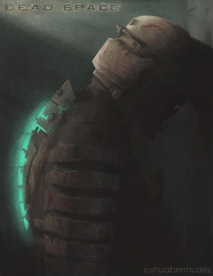 simple USB LED strip and it was done. i used this LED strip...
Dead Space Marker lamp
thingiverse
https://youtube.com/shorts/9rbez5RPx9Y?feature=share
Dead Space Marker iPhone 6 Case
thingiverse
Simple iPhone 6 case with a Marker design from Dead Space Print Settings Printer: Monoprice Maker Select v2 Rafts: Doesn't Matter Supports: Yes Resolution: .1 mm Layer Infill: N/A Notes: ABS Plastic, 245 degree Extruder, 90 degree print bed
Dead Space 2 Marker Redux
thingiverse
Dead Space markers are made up of many non-planar quads. The triangulation required for 3d printing results in some nasty undesirable, and inconsistent creases.
For this remix the model topology has been manually un-triangulated and cleaned up to...
The triangulation required for 3d printing results in some nasty undesirable, and inconsistent creases.
For this remix the model topology has been manually un-triangulated and cleaned up to...
Dead Space 2 Marker
thingiverse
Marker mesh extracted right out of Dead Space 2 data files, converted to STL, and flattened on the base for better printing and free-standing. Seen here next to a wiimote and a test print of the contact beam. The basis for this mesh is the property...
Stand for Dead Space 2 marker
cults3d
... original model. ... Features one 5mm hole for the LED in the middle of the Marker mounting base and another 5mm hole in the side for wiring. I wired mine to work from USB power. ...Bottom lid can be secured with two M3 screws or just glued to place.
Stand for Dead Space 2 marker
thingiverse
... original model. ... Features one 5mm hole for the LED in the middle of the Marker mounting base and another 5mm hole in the side for wiring. I wired mine to work from USB power. ...Bottom lid can be secured with two M3 screws or just glued to place.
Dead Space 2 Marker Keychain
thingiverse
You need the raft because it cant balance on the keychain part although you can make it small, mine was 5mm extra margin. I suggest tree supports with 1mm diameter if your using Cura, they are skinny enough to snap off so they dont get stuck inside. ..
..
Marker of Dead Space Free 3D print model
cgtrader
This is an HIGH FIDELITY miniature of the marker of Dead Space saga. In the game, the marker talks to people, leading them to madness. The first marker was found in the planet Aegis 7, by archaeologists of the Ishimura(space ship class "planet...
28mm Dead / Casualty Space Raider Centurion Miniature Marker
cults3d
Dead / Casualty Space Raider Centurion Soldier The alive one here : https://www.thingiverse.com/thing:3997251 more poses and builder packs here ..... ... Support Patreon : https://www.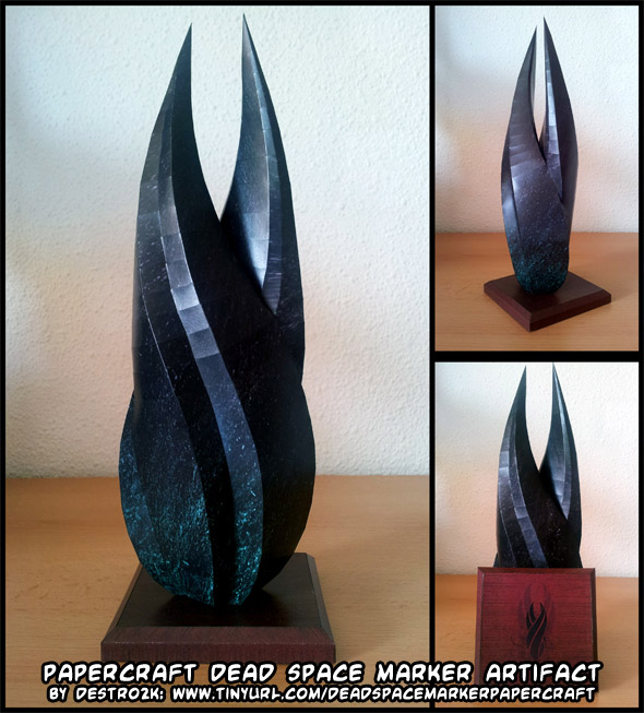 patreon.com/bigmrtong Patreon Preview : https://tinyurl.com/bigmrtong...
28mm Dead / Casualty Space Raider Centurion Miniature Marker
thingiverse
Dead / Casualty Space Raider Centurion Soldier The alive one here : https://www.thingiverse.com/thing:3997251 more poses and builder packs here ..... ... --------------------------------------------------- Support Patreon :...
Dead Goblin Skull Marker
thingiverse
So your PCs know when they are tripping over dead goblins and when they are tripping over prone goblins. ...Enjoy
Dead Space - Necromorph
thingiverse
from Dead Space
Dead space key ring
thingiverse
game merch dead space
Coffin (From Dead Space)
thingiverse
The coffin from Dead Space 3.
Isaac - Dead Space Pose1
sketchfab
TO PRINT 3D- ISAAC DEAD SPACE - HIGH QUALITY
Dead Space Helmet
sketchfab
High poly helmet from the game Dead Space.
Dead Space Isaac Bust
thingiverse
Isaac from Dead Space Bust for your printing pleasure
dead space statue
thingiverse
an easy to print statue from the video game dead space.
Pulse Rifle Dead Space
sketchfab
Here is the Pulse Rifle from Dead Space. ...Exercice for school.
dead space statue
myminifactory
an easy to print statue from the video game dead space.
Supportless Dead Space Soldiers
thingiverse
BLOOD FOR THE BLOOD GOD! ...Dead Space Marines that use 0 support!
Weapon Of Dead Space
sketchfab
Dead Space, I love this game designing, so I choose the weapon in it than make it !
Isaac Clarke - Dead Space
pinshape
3D printable model of Isaac Clarke from the video game Dead Space. Print with support settings activated. ...Always check the layers before printing.
Isaac Clarke - Dead Space
thingiverse
3D printable model of Isaac Clarke from the video game Dead Space. Print with support settings activated. ...Always check the layers before printing.
Federal State Budgetary Institution "National Medical Research Center for Eye Diseases named after Helmholtz" of the Ministry of Health of the Russian Federation
- Telemedicine
- Our doctors
- Schedule
- Write a letter
- Address
Moscow, Sadovaya-Chernogryazskaya 14/19
+7 495 625 87 73
- Events
- Contacts
- Events
- Contacts
- Structure
- History
- Employees
- Telemedicine
- Medical tourism
- Reviews
- Vacancies
- Legal Information
- Anti-corruption
- Office hours and hours
- Rules and regulations
- Appointment (adults)
- Appointments (children)
- Medical assistance
- Legal Information
- Paid services
- Questions and answers
- Chief Freelance Ophthalmologist of Russia
- WHO
- ABO
- Trade union
- Chief freelance ophthalmologists of Russia
- Russian Pediatric Ophthalmology
- Russian Ophthalmological Journal
- Ophthalmic portal Organ of vision
- Dissertation Council
- LEK
- Patents
- Clinical studies
- Young Scientists Council
- Department of Education
- Information about the educational organization
- Residency
- Postgraduate
- Advanced training
- Department of Continuing Medical Education
- Department of Eye Diseases FDPO MGMSU
- Methodological Accreditation and Simulation Center (MASC)
- media about us
Driving directions More
Moscow, st.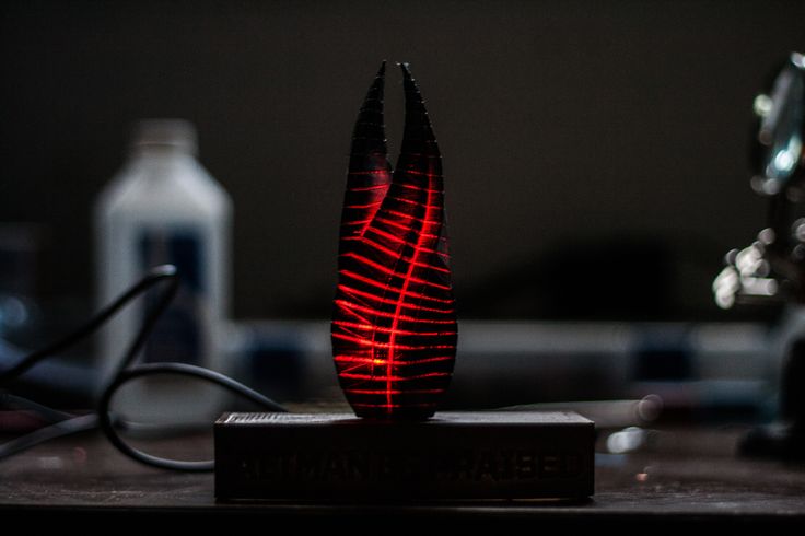 Sadovaya-Chernogryazskaya, 14/19
red gate
Moscow, st. Suvorovskaya, 35
Preobrazhenskaya Square
- Main
An error occurred while processing your request.
Back to main page
Helmholtz”of the Ministry of Health of Russia
Medical tourism
Highly qualified ophthalmological care for foreign citizens in accordance with international standards.
Printed circuit boards using a photopolymer 3D printer / Sudo Null IT News
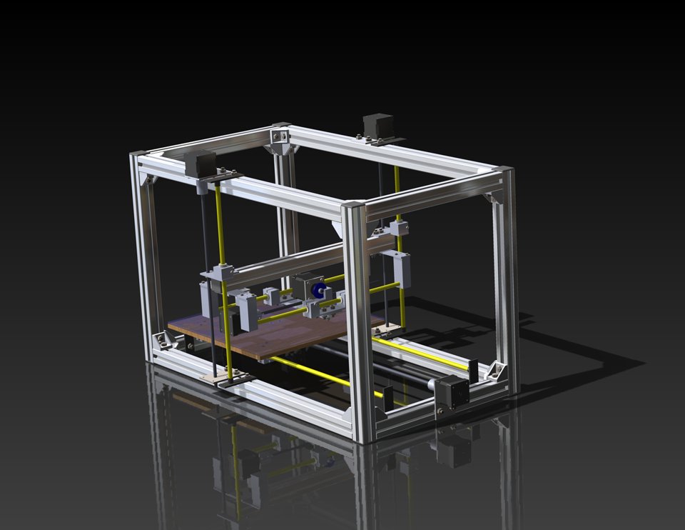
3D printers no longer surprise anyone. And in the last year or two, thanks to a strong reduction in cost, their photopolymer subspecies is also flourishing. Now such a printer is already available to almost everyone, and the number of their models on the market is multiplying every month.
Even when I just learned about the appearance of a new type of photopolymer printers a few years ago - in which the image of the layer for illumination is formed by an LCD, the thought “Hmm, what if we substitute a photoresist on a textolite for them?”. But then it was a purely theoretical question - the prices for them were considerable, and the resolution and display area left much to be desired. However, today these printers can already boast of a decent resolution - from 30 microns per pixel, and a completely normal display area.
And as it turned out, using an inexpensive modern photopolymer printer, it is quite possible to make boards with tracks / gaps from 0.15 mm.
I apologize in advance for such a voluminous graphomaniac, I myself did not expect that the note would get so fat...
I foresee the question "But why? In China, they will make normal boards with a mask and silk-screen printing for a penny!" I answer: now, most likely, there will be several iterations of finishing the board to a satisfactory state. I made a board - tested it - made corrections. And so several times. Waiting every time for 2-3 weeks from China is not an option :) But when the final design of the board is determined - then, of course, normal production in China or on Rezonit.
Now let's get down to business.
Who does not know - here is a brief principle of operation of such a printer The main part of such a printer is an LCD display. Below this display is a 405 nm UV source. Above the display is a bath of photopolymer, which has a thin transparent FEP film as a bottom. A platform is lowered into the bath, on which the model is “grown”. At the beginning of printing, the platform lowers to the height of one layer from the film, the image of the first layer is displayed on the display, and UV illumination is turned on for a specified time. Illumination, getting through the "open" pixels of the display and the film onto the photopolymer, hardens it, so a hardened layer is obtained. The first layer sticks to the platform. Then the illumination is turned off, the platform rises to the height of the next layer, the image of this layer is displayed on the display, and the illumination is turned on. The second layer is cured by welding with the previous layer. And this is repeated over and over until the entire model is printed.
The idea to try to make a printed circuit board using such a printer came to me again about three years ago, when I bought myself an Anycubic Photon S printer. , then I just forgot about this idea, because and there was no need to make boards. But the other day, the need arose for the manufacture of several small boards, and with a high probability that as tests are made, changes will be made to these boards and it will be necessary to go through several iterations of "manufactured-checked-changed" in a short time. And the idea resurfaced.
To be honest, I thought that by now the Internet would be filled with the results of such experiments, the idea lies on the surface :) But to my surprise I found that the Internet is almost completely silent on this issue. There are separate notes, but there is no integrity and completeness in them. That's why I decided to publish this post - maybe it will help someone go all the way faster than me, and with fewer rakes :)
Well, the most important thing is that you don't need a film and you don't have to struggle with increasing the contrast of the template. You also do not need a separate UV source with a place for its installation. And, of course, it is stylish, fashionable, youthful.
There are also disadvantages - the resolution of most modern 3D printers still does not cause much enthusiasm yet - the pixel size of all fluctuates around 0.05 mm. But this is already enough for confident manufacturing of boards with tracks from 0.2 mm and rather high chances of success with tracks from 0.15 mm. Due to the raster nature of such a template output, the position and size of elements on it can vary + -1 pixel, so I think it’s not even worth counting on tracks of 0.1 mm or less.
Let's go in order.
Problem
You need to make a printed circuit board at home using photoresist. Instead of templates and illumination lamps, use a photopolymer 3D printer that will serve both at the same time.
Let's divide the problem into separate steps-solutions for each moment.
-
Development of the board
-
Printer-friendly output of layers
-
Preparation of textolite with photoresist
-
Printer backlight
-
Photoresist development, board etching
1.
 PCB development
 Well, there are no questions. Whoever prefers to work in what program - in that one makes boards. The main thing is that the program should be able to display the result in some commonly used form. The easiest way I've come up with is outputting board layers to gerber files that can be fed to an online service. But you can also output to PDF or images.
2. Converting the CAD output to a printer friendly
This is where the trouble starts. If almost all CADs can output to generally accepted formats - gerberas, DXF, printing to PDF, then 3D printer manufacturers so far categorically refuse to accept any file standard. Everyone is perverted as they can. The situation is largely saved by the fact that many manufacturers use motherboards from one Chinese company, Chitu Systems, in their printers. Thanks to this, many printers on such boards are able to understand one of the basic formats developed by the same company. And even often, if a file has some unique extension, then in fact it has the same basic format, just with a different extension. But it may differ in some details.
In any case, there is a free UVtools utility known among photopolymerists that can open files in one format and convert them to another format. It understands almost all formats on the market :)
I have tried two ways of preparing files with layers for the printer and I will describe both.
2.1 Gerber output and conversion to .photon
The .photon file format is understood by the old Anycubic printers - Photon and Photon S. This is exactly the case when the printer manufacturer took the format from Chitu and changed its extension. In the original, this is the Chituvian .cbddlp format, so you can safely change the extensions of these file types among themselves and the printers will devour them like native ones.
Since I have a printer that understands this format, this method suited me perfectly. The limitations of this method are that the printer must understand .photon or .cbddlp files and have a display standard for most non-monochrome printers with a resolution of 2560x1440 and a diagonal of 5. 5". manuals on how to do this for any CAD that can, in principle, mirror layers or not - it makes no difference, they can be mirrored in the utility during the conversion process.0015
Now open the online utility for converting gerber files - https://pcbprint.online/ and load the gerberas into it. By the way, this is a utility from a Russian developer who lives here.
It is easy to understand, although it does not contain any information or help. But I will give a short guide:
For a single-sided boardUpload your gerbera in the main window with the "Upload file" button:
We made sure that everything is fine and the image meets expectations, if necessary, make a negative or mirror the image with the buttons in the top center, and press the button " Render layout":
Now press "Lauout" at the top right and get into another screen:
Here you first need to go to the settings (gear button at the top right) and there select the format of the output file "photon":
The time in "Exposition" can be left at default and change it to the desired one directly in the printer. But you can immediately put the right one if its value is already known :)
Close the settings and return to the previous screen. Here the output image is on a black space showing the working field of the printer. The image can be moved, aligned. When everything suits, we first press "Render", and when the "Download result" button next to it becomes active, we also press it. And save the proposed .photon file to a convenient location on your computer :)
For double-sided boards, things are a little more complicated due to the need to match them. Therefore, it is necessary to know very exactly the position of the image displayed on the printer's display in order to place the board on the display very accurately in accordance with it.
I had several options for solving this issue, but in the end I decided on the simplest of them, which did not require any mechanical conductors. To do this, I still in CAD in a separate layer (it is possible in the border layer or in any other "unnecessary" layer) I draw a frame around the board with a line of 0.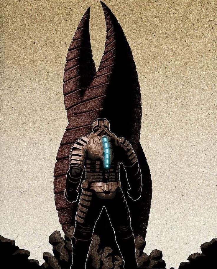 15 mm and indented from the edges of the board by 0.25 mm. As a result, I get three gerberas - the top layer, the bottom layer and a separate empty frame.
I upload all three gerberas to the above site and then in a few steps I get three files for the printer.
Double-sided board in pcbprint.online/So, all three gerberas have been loaded. All of them are mixed together, but it's not scary:
Now hide the top and bottom layers, leaving only the frame (by clicking on the eyes in the names of the gerberas).
Click "Render layout" and go to the "Layout" screen with the button in the upper right corner. We see an empty frame, drag it to the desired position on the black field of the display, click "Render" and "Download". The first file for the printer is ready.
Switch back to the gerbera screen with the "PCB comose" button. Redisplay the first layer (the frame layer still remains visible), mirror if necessary, and click "Render layout" again. Again we go to the output screen and now there are two pictures hanging on the display field - a separate frame and the first layer with a frame. The frame remained in the same place where we pulled it last time. And now our task is to exactly combine the frame of the first layer and the empty frame:
Click "Increase" and combine in one of the corners. In this case, in no case should you move the empty frame that we set in the last step!
Combined, click "Render" and "Download", and we have a second file for the printer. Before returning to the gerbera screen, we delete the render layer with the frame, we should again have an empty frame. And now we return to the gerberas, hide the first layer and display the second one, look at the need to mirror, click "Render layout" and go to this screen again. In the same way, we combine the layer frame with an empty frame (which cannot be moved!), then "Render" and "Download".
Everything, all three necessary files for the printer are ready.
All this hemorrhoids allows you to generate files for the printer of an empty frame and layers with a frame in the same place on the printer display with high accuracy. The empty frame serves to aim the board, more on that below.
If necessary, the resulting .photon files can be converted to the desired format using UVtools :)
2.2 Output layers to PDF or images
The second method is perhaps more confusing, but its great advantage is versatility, it is suitable for any printers, whose formats are supported by UVtools. I will describe it only in general terms, because. There are quite a lot of tools and specific ways to implement it, and everyone can choose them according to their preferences.
So, the goal of the first step is to get a picture with a size equal to the resolution of the printer's display, preferably in a lossless compression format. In this case, the image of the layer in the picture must correspond to the real size in the scale of the display.
If CAD allows you to output directly to the picture - great, output to it. If the resolution of the output image is configurable - specify the resolution of the printer display. It is elementary to calculate it - we divide the number of pixels across the width of the display by the width of the working area in mm and multiply the result by 25.4, we get the resolution in pixels per inch. If the resolution is not set, then set the image size as large as possible so that there are at least 15-20 pixels per 1 mm of the board.
If CAD image output is not available, output to PDF. This PDF will need to be opened in another program and converted to an image. Photoshop, Corel, maybe other programs can do this... The requirements for image resolution are the same. For example, in Photoshop, when importing a PDF, you can immediately specify with what resolution to convert to an image. For example, for common displays with a resolution of 2560x1440 and a diagonal of 5.5 "the resolution is approximately 537.566 PPI (pixel size - 0.04725 mm).
The resulting image will need to be changed in some image editor, bringing its size to the resolution of the printer's display. In this case, the layer image must be scaled to the real one (taking into account the pixel size of the printer display) or saved without scaling if the PPI of the display was specified when importing the image.
UPD: in the comments @0x3f00 gave a link to his converter of PNG images to files for the .photon printer - https://github.com/0x3f00/PhotonCpp/releases/tag/v1.0.0 . There is also an instruction for using it just for the purpose of manufacturing boards - https://github.com/borelg/PhotonPCB.
2.3 There is another way, but it is very resource-intensive
You can output layers to PDF, then open this PDF in Corel, convert it, save it in DXF, extract a three-dimensional object from this DXF, which you can push into the printer's slicer.
Necessary transformations in the vector editor:
-
Connect all curves.
-
Convert outlines to objects.
-
Merge intersecting objects.
You can extract a three-dimensional object from DXF, for example, in SolidWorks. Fusion360 also seems to be able to. Who else is capable of this - I honestly don't know, but in theory any CAD that can import DXF as a sketch.
Thus, for example, I made a model for determining the exposure time of the photoresist.
3. Preparation of textolite with photoresist
The Internet is littered with articles on this topic, but for the sake of integrity and for the sake of some specific points, I will also describe such well-known stages as the preparation and etching of textolite.
My first experience of such manufacture was a couple of days ago with a domestic photoresist PF-VShch. Taking into account the last yesterday's experience, I categorically advise not to waste time on this photoresist, but immediately take a decent one - Ordyl Alpha 350(330) :) They say that Kolon is also decent, but I have not tried it. With Ordyl photoresist, the results are much more stable and accurate, it is easier to develop and adheres much better to the foil. And he can forgive those mistakes that will be critical for the PF-VSC. And what is important - it is sold in a bunch of places quite inexpensively.
3.1 Preparing the textolite
To begin with, the textolite should be smooth, very preferably with a smooth foil without scratches or dents. Otherwise, the chances of success are reduced.
If a double-sided board is being made, then you need to immediately cut the board out of the PCB exactly to size. If there is any CNC router, then you can drill all the holes and cut along the contour in one installation, as I do. If not, then it is better to leave the drilling for later, when the board is etched.
After this, the textolite blank must be cleaned and degreased very carefully. This can be done with a kitchen abrasive sponge (but not used for washing dishes on which fats have already accumulated) and a scouring powder like Pemolux. Very carefully, slowly three every square millimeter of foil, without touching it with your fingers. In general, I categorically do not advise touching the foil with your fingers after the start of cleaning, there should not be the slightest even the faintest greasy spot on it. After cleaning, rinse thoroughly in running water, shake off excess water and allow to dry. I do not advise blotting or wiping with anything, because. grease can be applied, even from a new napkin.
3.2 Application of photoresist
Also a fairly common topic on the Internet, so I'll go over it briefly.
Photoresist usually comes in sheets or rolls. It consists of three layers - two protective films and the photoresist itself between them. A piece is cut off from the photoresist according to the size of the board + 5 mm in length and width, then a matte (polyethylene) protective film is removed from it.
the second, glossy (lavsan) must remain on it until the etching stage.
The easiest way to remove the film is with a piece of tape. It is glued with its edge to the corner of the photoresist and then folded back, pulling the protective film along with it.
After removing the matt film, the photoresist is applied to the edge of the board and smoothed along this edge with a finger. The rest of the photoresist is supported by weight, without tension, but in such a way that as little as possible of its area lies on the foil.
Please note that if Ordyl photoresist falls on a well-prepared textolite, then it can stick tightly to it, and you won’t roll it without bubbles. You have to scrape it off and do it all over again. And PF-VShch can fall as much as you like - it definitely won't stick :)
Now the knurling itself. If you have a laminator, in which the textolite will crawl through the thickness, then it's just wonderful. We make an envelope-type strip of paper folded in half, put a textolite with a sticky edge of the photoresist in it, and serve this sandwich into a laminator heated to 100-110 degrees. At the same time, we continue to hold the photoresist so that it comes into contact with the textolite foil only directly at the inlet of the laminator.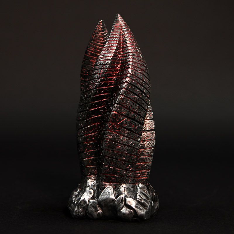
That's all for Ordyl, for PF-VShch it will be harmless to roll a couple more times.
If there is no laminator, then smooth the photoresist to the textolite with your finger from edge to edge, gradually lowering it onto the textolite. The main thing is not to catch the bubbles. After all the photoresist lay on the foil, we take a hair dryer and heat the textolite to 70 degrees, after which we iron the entire photoresist once again.
After knurling, let the textolite with photoresist lie down for 15-20 minutes, or at least until they cool down to room temperature - according to the recommendation of the photoresist manufacturer.
And now everything is ready to highlight the layer pattern :)
4. Printer highlights
I want to warn you right away: looking directly into the glowing display of a photopolymer printer may not be very good for the eyes. Although not true UV (405 nm), the brightness is quite noticeable and can be harmful to the eyes.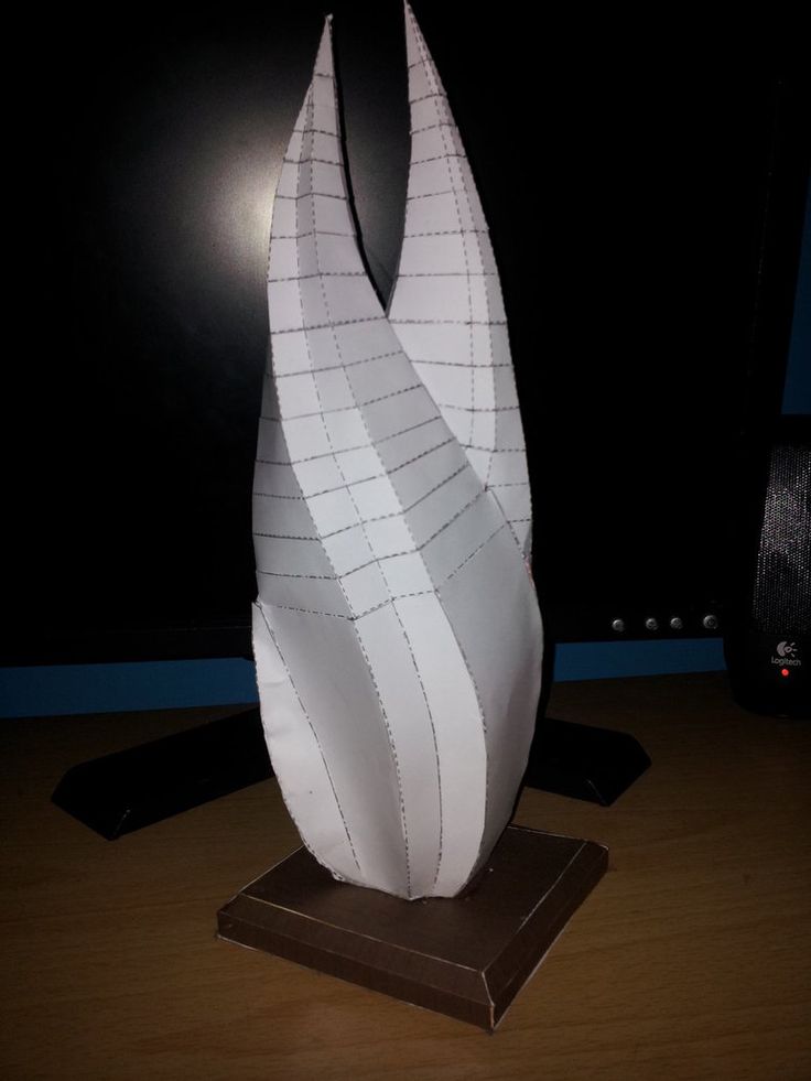 Therefore, I recommend using colored or tinted goggles. I think even sunscreen will do.
First, you need to remove the bath and platform from the printer, they are completely unnecessary for this business and even interfere. This completes the preparation of the printer :)
Lighting also has different options. If you have a one-sided board and the blank is larger than the size required for the board, then everything is simple - throw the file obtained at the preparation stage into the printer and, knowing the approximate place for displaying the image on the display, put a textolite with photoresist in this place. Then start printing the file and wait until it is completed. Everything, the photoresist is exposed, it is possible to develop.
If the workpiece is equal in size to the board being made and the error with the position of the workpiece on the display is unacceptable, then in this case it is necessary to remove the frame during preparation, as is the case for a double-sided board.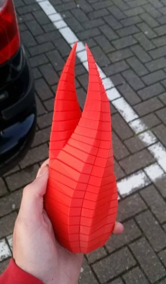 Illumination also occurs using a frame, similar to a double-sided board, only without the second side and the second layer.
So, the illumination of the double-sided board. We throw all three files into the printer - with a frame, with the first layer and with the second layer. We put the workpiece next to the printer in quick accessibility. If it is already pre-drilled, it will be useful to make sure that it lies in the correct position so that you can quickly take it and immediately put it on the display. To do this, we run a file with a layer planned for exposure, and compare the layer pattern on the display and the orientation of the board next to the printer.
Printing a file with one frame. As soon as the frame lights up on the printer display, we take the workpiece and put it approximately inside the frame. While the frame is being illuminated, we align the workpiece so that it is exactly in the frame, with the same indentation of the frame from the edges of the workpiece on all sides.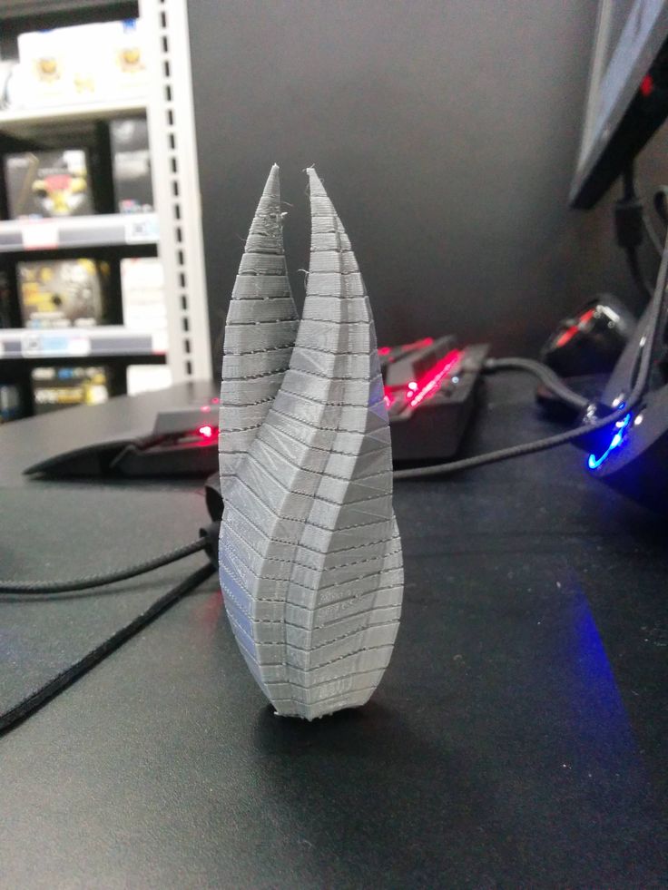
In the photo, I gave an example with a ready-made board, because I did not take pictures during the manufacturing process. Well, reflections interfere quite strongly, alas... But I think it's understandable :)
That's it, the position of the workpiece is verified, printing of the frame file can be interrupted or wait for it to finish. Without moving the workpiece, run the file with the first layer and wait for it to finish. We illuminate the second layer (the second side) in the same way - we launch the frame, place and align the workpiece, without moving it, we launch the second layer. Before this, just in case, you can make sure that the workpiece will lie in the correct orientation, as before the first layer.
If the workpiece is not completely flat and does not fit the entire area of the display, then you can press it down from above with some heavy flat piece of iron. You just need to make sure that this piece of iron does not interfere with the platform lever, which will go down with the start of printing - the printer thinks that this is a normal photopolymer print and you need to lower the platform to the bottom of the bath :)
Illumination time can be different from printer to printer .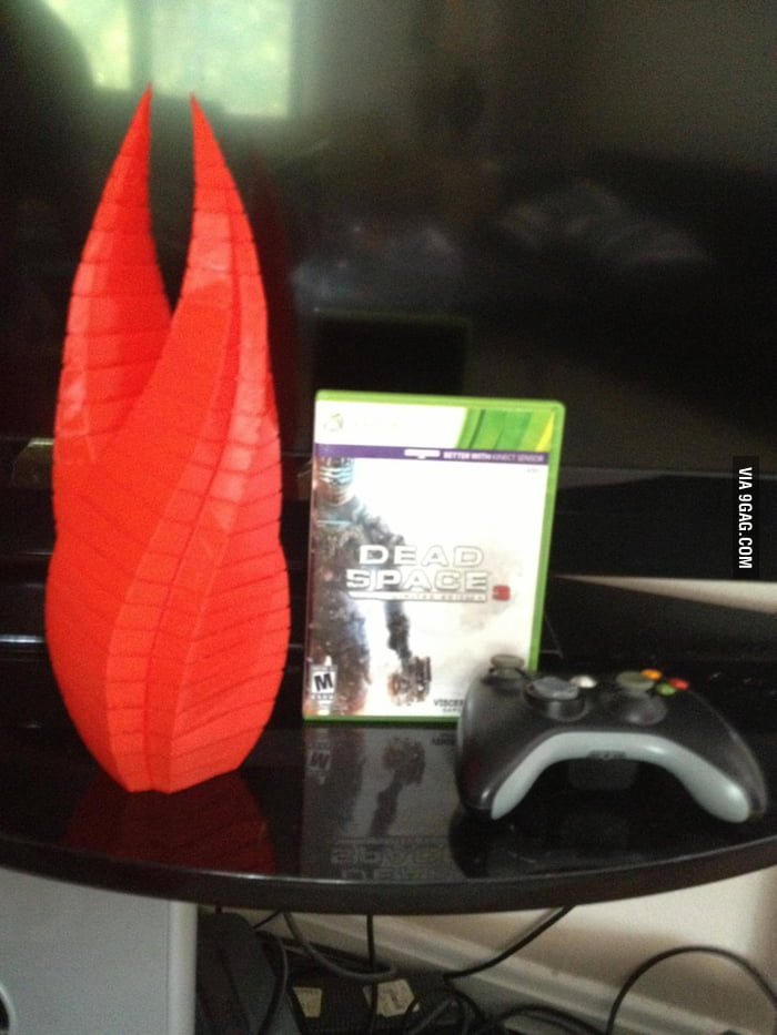 It depends on the power of the emitter, and on the optical illumination system, and on what type of display is worth - monochrome or RGB. Here already it is necessary to select each individually. For orientation, I can say that I got the best result with the Ordyl photoresist at an exposure time of about 90-110 seconds. With photoresist PF-VShch - about 10-13 minutes. Printer with paraled, illumination power slightly less than 50 watts.
After exposure, the workpiece should be allowed to rest for 15 minutes - this is according to the recommendation of the photoresist manufacturer. Ordyl changes the color of the highlights quite noticeably, so it's pretty easy to control the highlights. Unfortunately, the photo did not convey it well, it can be seen better with the eyes.
5. Development, etching
Everything here is according to the recommendation of the photoresist manufacturer and according to the classics of the Internet.
All necessary chemicals were purchased inexpensively from Auchan. Even hydrogen peroxide 6% - this was a surprise for me, I had never seen it in hypermarkets before, and even in liter bottles.
For one session you need:
-
Soda ash - 1.5 grams
-
Hydrogen peroxide - 150 ml for 3% (or 75 ml for 6% + 75 ml of water)
5 gram -
Salt - 7.5 grams
-
Alkali (caustic soda, sodium hydroxide) 5-7% - 100 ml
With the cheapness and ease of buying all the components around the corner, I am in favor of preparing a new solution for each board. Although the etching solution, as they say, is not stored anyway. A solution of soda ash noticeably "poorer" in the process of development. Unless caustic soda can be reused, but is it worth it to keep another bottle ...
Both Ordyl and PF-VShch appear in a weak solution of soda ash. For PF-VShch - 1-2%, for Ordyl - 0.8-1.2%. For Ordyl, we take 150 ml of water and dilute 1.5 grams of soda in it. The solution can be heated up to 30 degrees, this will speed up the development, but it is important not to overdo it, otherwise the illuminated areas may begin to be damaged.
Ordyl appears rather quickly. Already after 10-15 seconds, the illuminated pattern begins to become more and more contrasty, the unexposed areas gradually dissolve, become thinner and become paler.
To speed up the process, it is recommended to shake the bath so that the reaction products are washed off the surface of the workpiece. For this I adapted my old 3D printer, its table and shook and heated the bath with the solution during development and etching :) Two minutes passed before there were at least some signs that development had begun. In addition, if Ordyl does dissolve, then PF-VShch first swelled like gelatin and discolored, and only then began to slowly dissolve.
At the end of development, you can go over the boards with a hard paintbrush (or soft toothbrush) several times in different directions to help wash out any remaining photoresist from tight spots. Ordyl holds on tight, this procedure should not disrupt it, but with PF-VShch you need to be very gentle, even without a brush it strives to exfoliate on thin paths.
After etching, the workpiece must be rinsed in cold water so that the soda residues do not continue to attack the photoresist and so as not to clog the etching solution with them.
The result should be something like this, maybe even better :)
More detailsGrid square scale - 0.2 mm:
The scale is the same. Here you can see the raster component of the illumination, the pixels stick out:
Etching was also done according to the traditional recipe, popular on the net:
It is better to heat the solution to 40-50 degrees, then the etching goes much faster. This is my first experience with this solution. I used to poison with ammonium perchlorate, and even earlier - with classic ferric chloride. To be honest, I can't really express how I feel about this solution. On the one hand, it poisons rather quickly, is transparent, does not get dirty, and is relatively safe. On the other hand, it seemed to me that it was easing quite a lot ... But maybe it just seemed, I haven’t been making boards for 10 years and I forgot how it all worked when the trees were big :)
After etching, the exposed photoresist must be removed from the workpiece, and this is done in caustic soda.
 On my bottle of cleaner it says "at least 5% but not more than 15%" and it takes 5-8% to remove the photoresist. I diluted the product 1:1 with water and this solution did the job perfectly. The photoresist does not dissolve in it, it simply peels off the foil after 2-3 minutes and begins to float in tatters in the solution.
 After that, the board is thoroughly rinsed under the tap and... The board is ready!
Summary of my experience
In general, I am satisfied. I did not expect to get tracks / gaps of 0.1 mm and I did not get them. Here, the capabilities of the printer are severely limited (pixel size), and in general, good experience is needed for such results. But I was hoping to get at least 0.2 mm, and if I'm lucky, then 0.15 mm - and I got it. 0.2 mm confidently, 0.15 mm - well, so-so... If you try, you can achieve :)
There were some flaws - it was not pickled in some areas, and imperfect alignment of layers and holes. But neither is critical. As for the non-mordant - I think that I just hurried to take it out of the developer, I was afraid after PF-VShch that thin paths would begin to peel off.
Learn more