3D print microfluidics
3D printed microfluidic devices: enablers and barriers
Sidra Waheed,ab Joan M. Cabot,ab Niall P. Macdonald,ab Trevor Lewis,b Rosanne M. Guijt,c Brett Paullab and Michael C. Breadmore*ab
Author affiliations
* Corresponding authors
a
Australian Centre for Research on Separation Sciences (ACROSS), School of Physical Sciences, University of Tasmania, Hobart, TAS, Australia
E-mail:
mcb@utas. edu.au
Fax: +61 3 6226 2858
Tel: +61 3 6226 2154
b ARC Centre of Excellence for Electromaterials Science (ACES), School of Physical Sciences, University of Tasmania, Hobart, TAS, Australia
c Australian Centre for Research on Separation Sciences (ACROSS), Pharmacy School of Medicine, University of Tasmania, Hobart, TAS, Australia
Abstract
3D printing has the potential to significantly change the field of microfluidics. The ability to fabricate a complete microfluidic device in a single step from a computer model has obvious attractions, but it is the ability to create truly three dimensional structures that will provide new microfluidic capability that is challenging, if not impossible to make with existing approaches. This critical review covers the current state of 3D printing for microfluidics, focusing on the four most frequently used printing approaches: inkjet (i3DP), stereolithography (SLA), two photon polymerisation (2PP) and extrusion printing (focusing on fused deposition modeling). It discusses current achievements and limitations, and opportunities for advancement to reach 3D printing's full potential.
- This article is part of the themed collections: Lab on a Chip Recent Review Articles, RACI100: Celebrating Australian Chemistry, 3D Printing and Lab on a Chip 2016 Most Downloaded Articles
Researchers open up low-cost open-source microfluidics 3D printing
0Shares
A team of researchers from the University of Bristol has developed a novel low-cost and open-source 3D printing process for producing microfluidic devices.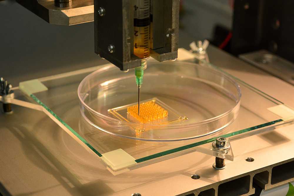
A microfluidic chip is a set of micro-channels etched or molded into a material, such as glass, silicon, or in this case, PolyDimethylSiloxane (PDMS), which are connected to the outside world by inputs and outputs pierced through the chip. Through these holes, liquids or gases can be injected and removed by external active or passive systems for biomedical field applications such as laboratories-on-a-chip (LOC), cell biology research, and protein crystallization.
Requiring only simple domestic equipment and a standard desktop 3D printer, and having been developed in free-to-use software, the researchers’ process reduces the cost and complexity of fabricating microfluidics to make the field more accessible.
The team believes their approach could drastically lower the threshold for research and education into microfluidics while making the rapid prototyping of affordable LOC diagnostic technology possible at the point-of-care (POC).
Proposed microfluidic master mould fabrication process. Image via University of Bristol.
3D printing and microfluidics
For decades, LOC technology has been heralded to answer a range of biological, chemical, and healthcare challenges. However, it is yet to see meaningful adoption and deployment due to the cost both at the research level and the mass-manufacturing stage.
LOC technologies are supported by the field of microfluidics, which is seeing an increasing exploration of 3D printing techniques to advance the technology and increase its accessibility.
In 2018, researchers from New York Genome Center and New York University developed an open-source 3D printed droplet microfluidic control instrument which was reportedly up to 200 times cheaper than other comparable instruments. Designed to identify and target the correct cells to treat diseases such as Rheumatoid Arthritis, the instrument could be obtained and assembled for around $600.
Elsewhere, a process has been developed to 3D print microfluidic devices integrated with fluid handling and functional components.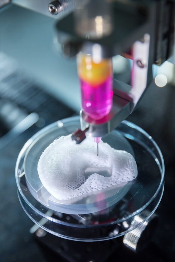 Developed by the Singapore University of Technology and Design, the technique aimed to enable the rapid prototyping of microfluidics for LOC applications in chemical testing and cell analysis.
Most recently, researchers from UC Davis unveiled a new approach to 3D printing using microfluidics, which involved deploying a droplet-based microfluidic system to efficiently 3D print finely-tuned flexible materials. Possible applications for the technology include soft robotics, tissue engineering, and wearable technology.
Material printed with UC Davis’ new droplet-based 3D printing method. Photo via Jiandi Wan.Fabricating the microfluidic devices
The researchers began by 3D printing interconnecting microchannel scaffolds with an Ultimaker 3 Extended 3D printer using PLA, which were then thermally bonded to a glass substrate in the desired configuration to create a microfluidic device master mold.
The microchannels were designed in a range of modular patterns, with each featuring interlocking ball-socket connector ends, using Ultimaker’s Cura open-source slicing software.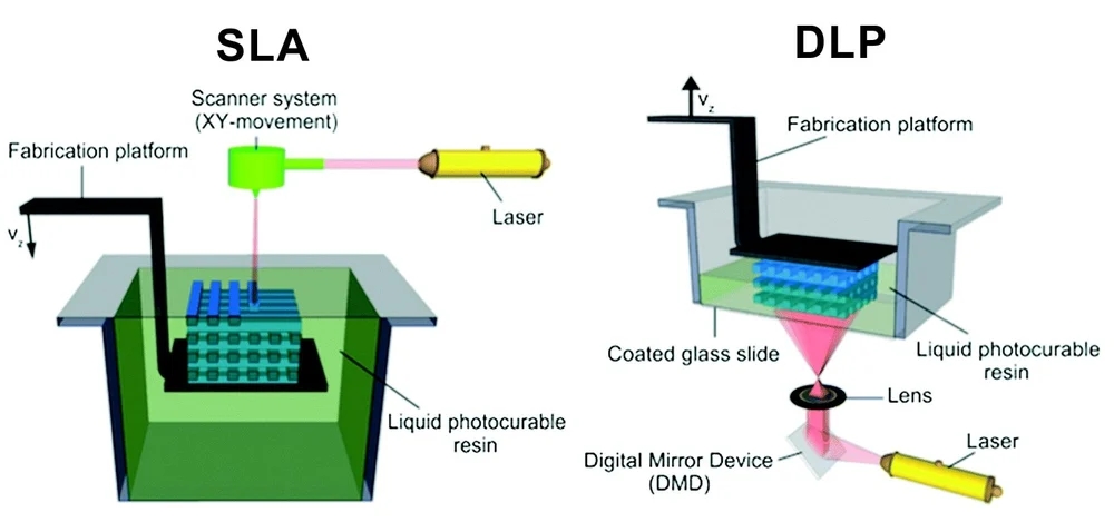 These ends were developed to mimic puzzle pieces. Successive modules could be arranged in any desired configuration, enabling creating more sophisticated microfluidic systems using a small number of simple modules. A key aspect of this part of the researchers’ process is that it is easy and clear to replicate for non-expert users.
The 3D printed microchannel modules were then mounted onto standard 1mm-thick glass microscope slides into the desired configuration, using the ball-and-socket connectors. The channels were then heated for around a minute to bind them to the glass with a weighted slide placed on top to prevent deforming and shrinking. After heating, the slides were partially fused and placed weighted-side down onto a metal plate to rapidly cool the weighted slide and remove it from the mold.
The master mold can be used again and again to produce microfluidic devices in PDMS. Post-printing, the master mold fabrication process can be completed in less than five minutes, allowing the method to be used for both formal and informal learning environments.
Open-source microfluidics
To ensure the proposed technique is fully democratized, the researchers developed an open-source Autodesk Fusion add-in which allows any user to design and export interconnecting microfluidic channel scaffolds for 3D printing. Using this plugin, a user can go from a microfluidic channel design to a completed microfluidic channel without requiring CAD software expertise or time and resource-intensive techniques or equipment.
Users can prototype interconnecting microfluidic channels down to 100 μm resolution in width, either through printing their own designs or choosing from a vast library of microchannel scaffolds listed in the add-in. A protocols.io instruction set has also been made available detailing the researchers’ full process, with links to the up-to-date add-in and profiles.
Using this technique, users can fabricate microfluidic devices from PDMS with only household equipment and no hazardous chemicals, thereby making microfluidic experimentation accessible to schools, hobbyists, and researchers no matter their resources. The team hopes that this approach will be adopted by researchers and educators worldwide to “help to inspire the next generation of lab-on-a-chip developers.”
Furthermore, the researchers believe their technique could pave the way for “truly affordable” LOC healthcare diagnostic testing, which can be performed at the point-of-care, through applying the microfluidic PDMS channels directly to any cleaned glass surface, such as a mobile phone screen or a car windshield.
Further details on the study can be found in the paper titled “Negligible-cost microfluidic device fabrication using 3D printed interconnecting channel scaffolds” published in the Plos One journal. The study is co-authored by H. Felton, R. Hughes, and A. Diaz-Gaxiola.
Subscribe to the 3D Printing Industry newsletter for the latest news in additive manufacturing. You can also stay connected by following us on Twitter and liking us on Facebook.
Looking for a career in additive manufacturing? Visit 3D Printing Jobs for a selection of roles in the industry.
Featured image shows proposed microfluidic master mould fabrication process. Image via University of Bristol.
Tags A. Diaz-Gaxiola H. Felton lab-on-a-chip Microfluidics New York Genome Center New York University R. Hughes Singapore University of Technology and Design UC Davis Ultimaker Ultimaker 3 Ultimaker Cura University of Bristol
Hayley Everett
Hayley is a Technology Journalist for 3DPI and has a background in B2B publications spanning manufacturing, tools and cycling. Writing news and features, she holds a keen interest in emerging technologies which are impacting the world we live in.
3D printing helps create record-breaking microfluidic channels
3D printing Physics Physicists were able
Complexity 3.3
3D printed microfluidic chip.
BYU University Communications
A team of scientists from Brigham Young University (USA) proposed a 3D printing method for creating microfluidic "laboratories-on-a-chip" with record thin channels. Thanks to DLP (“digital light processing”) technology and careful selection of the printing material, the authors achieved a 100% yield when creating channels with a cross section of 18 × 20 square microns - 10 times smaller than what has been possible so far. The study was published in a specialized journal on microfluidics Lab on a Chip .
Microfluidics is a field that studies the behavior of liquids in channels with a thickness of the order of microns. Due to their small size, microfluidic devices make it possible to carry out complex multi-stage manipulations with liquids and objects placed in them (cells, bubbles, particles, drops) using chips several millimeters in size. Hence the name of the most popular microfluidic devices - "laboratories on a chip".
Compared to macrosystems - the usual "pipes" and relatively thick (mm) capillaries - in microfluidics, the behavior of the liquid changes somewhat. For example, viscous resistance and surface properties play an important role. A separate problem is the production of thin channels, because, as in microelectronics, each chip consists of numerous "tracks" (channels for liquids) with "crossroads", valves and sections with a special shape and relief of the walls.
Soft lithography has traditionally been used to create microfluidic systems, but 3D printing has also gained popularity recently. However, until now, she lacked the accuracy and resolution to seriously compete with lithography. The authors of the new work created their own modification of a commercial 3D printer and selected a specific material for printing, as a result of which they were able to achieve a record resolution.
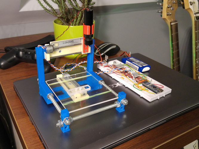
Diagram of the printer used in job
Hua Gong et al. / Lab on a Chip
Share
Wall materials in microfluidics are usually polymers, which are formed from a liquid solution during photopolymerization. To do this, each layer applied during printing must be irradiated with light with a certain wavelength. In this case, the illuminated sections of the layer will freeze and become walls, and the unlit sections will then be washed away, and in this place there will be a “void”, that is, the channel itself. In order to accurately illuminate only the required areas of the layer, the authors used the DLP method, which is widely used in projectors, both domestic and industrial. These devices have a system of prisms and mirrors that creates the necessary sequence of pixels in each image. The light source in the work was an LED with a wavelength of 385 nanometers, which is lower than the commonly used 405 nanometers - this allowed us to consider a larger range of materials suitable for printing.
The authors paid special attention to the light-absorbing additive, which solved one of the main problems of 3D printing of microchannels. Imagine that the printer has just printed a layer that has a void (channel) in it, and the next layer should be solid (top cover, for example). When illuminating a "pixel" located above the void, the light can penetrate the previous layer, resulting in a wall instead of a void. To avoid this, a photo-absorbing additive is added, which prevents light from penetrating further than required.
The photoabsorbing substance was selected by the authors from 20 candidates, which were compared according to 6 criteria: solubility in the base material, absorption spectrum (compatibility with a light source), critical temperature, mechanical strength after polymerization of the sample, fluorescence ability (parasitic and unnecessary in this work) and the print resolution provided, i.e. the depth of light penetration. After such selection, scientists left only one substance - NPS (2-nitrophenyl phenyl sulfide).
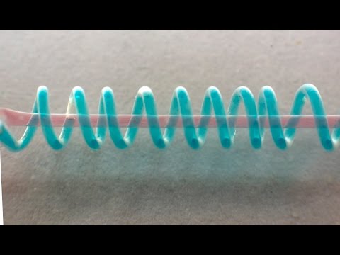
Example of printed serpentine channel
Hua Gong et al./ Lab on a Chip
Share
In order to test the finished method, the authors printed several typical microfluidic systems: a serpentine, as well as a channel with a large vertical aspect ratio - 25 microns wide and 3 millimeters high. Scientists also estimated the width of one "pixel" in the print plane - 7.6 microns, and the minimum achievable channel cross section was 18 × 20 square microns. The article notes that lithography methods can also achieve lower values, but they lack many of the possibilities of three-dimensional printing, for example, creating full-fledged 3D devices in which the channels do not lie in the same plane.
The range of applications for 3D printing today remains very wide: from microfluidics and organ printing to building construction.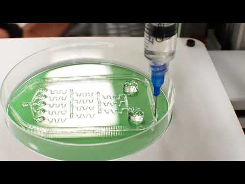 The range of materials used is just as wide: in addition to plastic, systems for printing with metal or glass are known.
Taras Molotilin
3D printing against COVID-19
You are here
Home
Increasingly, microfluidic chips are being used for medical analysis. These chips allow scientists and physicians to measure some kind of biomarkers (such as the content of certain proteins in the blood plasma) and use these data to study biological processes in a normal state, during an illness, or under the influence of drugs. From a technological point of view, microfluidics is a set of techniques that allow you to control the flow of small portions of liquid. Recently, these technologies have been used for the production of diagnostic medical devices. In such microfluidic chips, several different biological parameters can be measured in parallel, and this can be done quickly. Thus, it is possible to make devices, including for tests for coronavirus infection COVID‑19.
In any microbiological laboratory, there are always a lot of instrumental units connected to each other - and only if all the devices work in harmony, the laboratory will work properly. The ability to quickly change the characteristics of at least one of the instrument modules will save the laboratory millions of rubles, but replacing blocks at the instrument level associated, for example, with complex electronics or photonics, is very expensive and difficult. But adjusting the parameters of the microfluidic module by manufacturing new chips is both cheap and fast.
Elements with different functions can be combined on a single microfluidic chip for parallel analysis of multiple indicators. For example, on a chip for covid tests, some channels on the chip are needed for antibody transport, and others are needed to detect viral RNA. Thus, one small microfluidic device turns into a kind of microlaboratory (hence another name for the technology: “laboratory-on-a-chip”). With microfluidic devices, researchers can conduct biomedical analysis of large numbers of samples at high speed. However, until now, the methods of their production have had rather significant limitations, and the point is not only that their production by traditional methods is a very long and expensive process, but also that many products with a complex shape of internal channels are in principle impossible to obtain. using traditional methods.
Reducing the diameter of the channels and speeding up production
Photolithography is now most often used for the production of microfluidic chips. This technology has its drawbacks, in particular - the process itself is a large number of fairly complex manual operations. This feature can lead to defects in the geometry of the finished device and, accordingly, to problems with the reproducibility of the technique.
In addition, traditional photolithography is designed to create structures with a constant height, that is, all elements in a microfluidic chip are of the same depth and are in the same plane - this, of course, imposes restrictions on the chip architecture and reduces the variety of analytical capabilities of the final product. Another drawback of the technology is not very high resolution. Available devices for photolithography allow you to create reliable chips with channels with a diameter of about a hundred micrometers or more. In principle, thinner channels can also be obtained using photolithographic methods, but then the probability of defects in their structure increases and their correction prolongs the already long production process even more. Because of this, scientists are deprived of the opportunity to obtain more accurate and compact devices.
A new microprinting technology, projection micro stereolithography (PµSL), introduced in 2020 by Boston Micro Fabrication, has helped change the situation. Their microprinting setup makes it possible to create products with a size of several tens of micrometers with a resolution of 2 micrometers, while including internal channels and cavities of any shape in the chip architecture. Already in the first test chip printed using the PµSL technology, it was possible to make a channel with a diameter of 50 microns - this is half as much as it was possible to obtain before. As a result, on a microfluidic chip, which used to fit four channels, it was possible to make eight at once. The compactness of the device allows you to expand its capabilities, while not increasing, but, on the contrary, reducing the size. According to scientists, if you use the BMF S130 installation, the most accurate to date, then up to 20 channels with a diameter of 15 micrometers can be placed on a chip of the same size. In addition, 3D microprinting allows you to test various device variations and quickly make changes to the product design.
Speed of production - along with a wide variety of microchannel geometries and the ability to quickly correct them if necessary - is an important advantage of 3D microprinting. The technology of traditional photolithography at the first stage involves obtaining a mask for irradiation using high-precision expensive devices, and, as a rule, this alone takes at least a week. And the full production cycle of products takes a month or more. 3D microprinting technology also includes several post-processing steps, but even with this in mind, the researcher will be able to receive the finished product within a few days after the order. At the same time, most of the production stages are automated and do not require any human intervention.
Chip production using BMF3D technology
Thus, PµSL 3D microprinting technology allows you to make any products with micrometer precision without the need to order them from contractors, significantly reducing the risks associated with lengthening supply chains. Another advantage of the technology is significant cost and time savings, which are essential for advanced development. In addition, a five-fold increase in the number of microchannels in a fixed-size medical chip dramatically increases the potential amount of data that can be obtained on it. And the ability to go out of plane during 3D printing allows researchers to place channels on the chip in several layers, while controlling their shape and inclination.