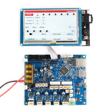
Duet 3d printing board
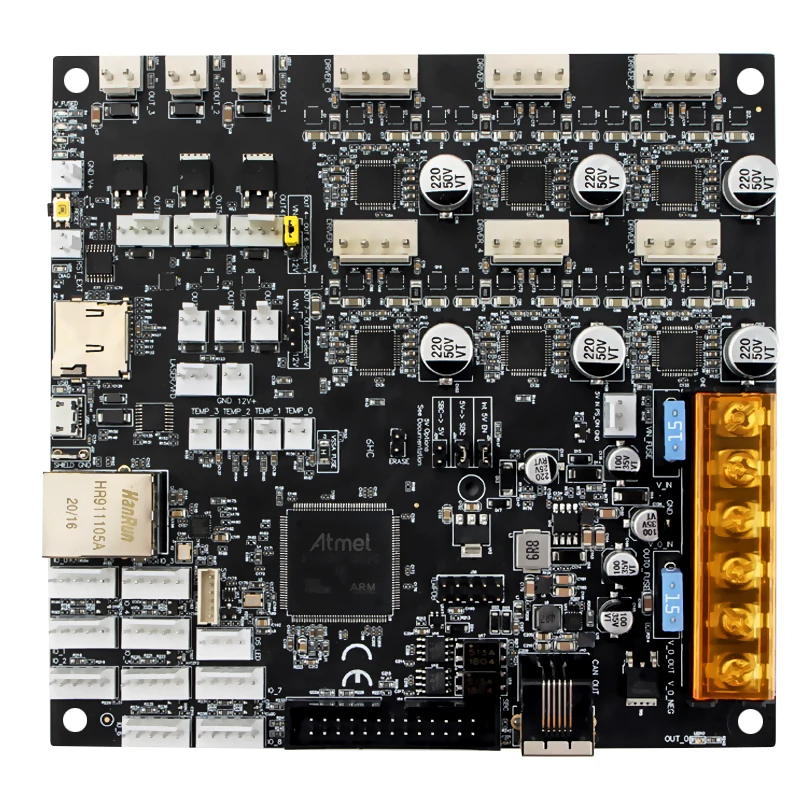
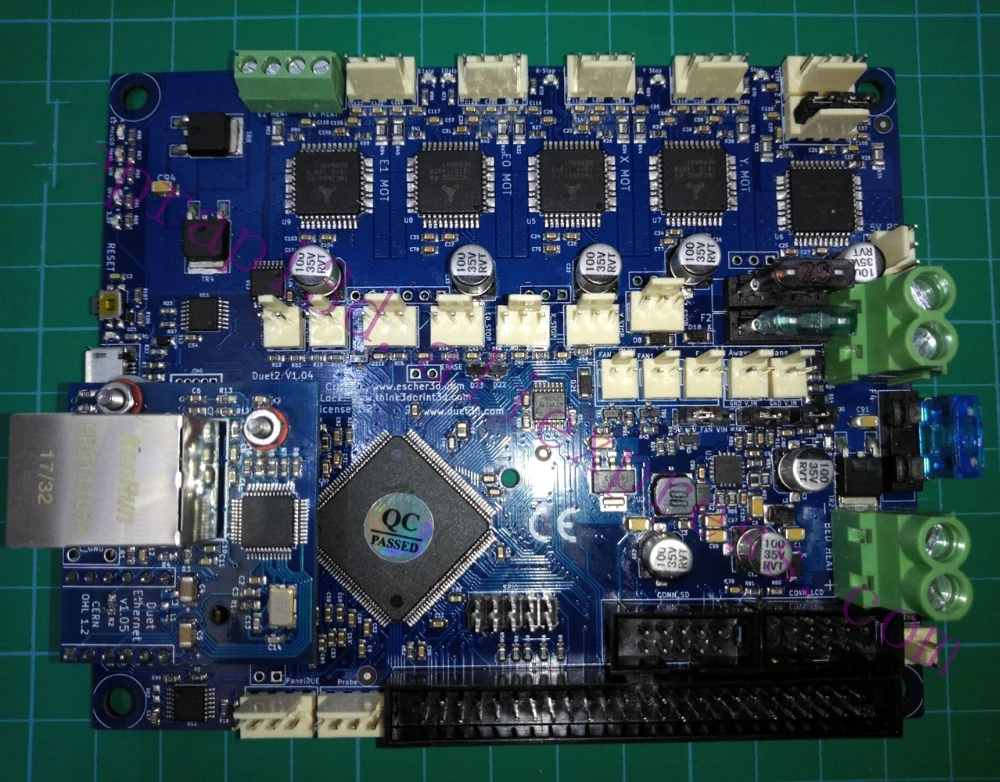
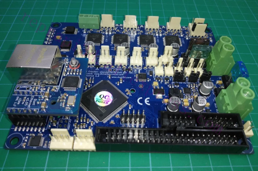
Duet3D Duet 2 Ethernet 3D Printer Controller Board
- Home
- Store
- 3D Printer Accessories
- 3D Printer Controller Boards
- TMC2660 Equipped Controller Boards
The Duet 2 3D printer controller board combines some of the best components available into an incredible all-in-one controller. Don't sweat which drivers to get - the TMC2660's come baked in and an onboard WiFi or Ethernet connection enables networked printing from anywhere on your LAN.
Current Version: v1.04
Remove from wishlist Add to wishlist loading...
Tagged: 3D Printer Controller Boards, 5 Stepper Max Controller Boards and RepRap Firmware Controller Boards
Product No. loading...
Notify me when this item becomes available Success You will be notified when ... becomes available.Everything you need in a controller
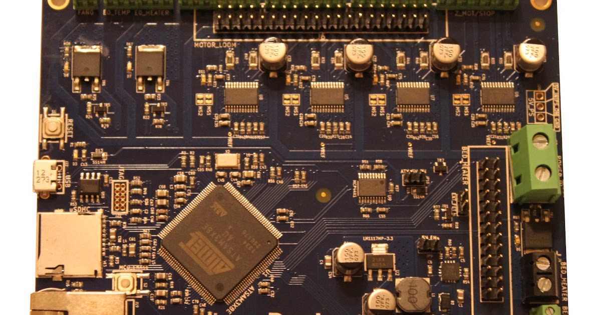
The Duet 2 provides fast motion and quick processing via a 32 bit processor. All that processing power means you can also expand your machine to include many more stepper drivers. (additional expansion boards may be required) Firmware is stored locally on a Micro SD card and can be accessed via the web interface for easy modification. Connections to all other hardware components is easy with vertical molex connectors or screw terminal block for secure connectivity.
And everything you want!
The Duet 2 includes a baked-in network chip for easy machine control from any device on your network. From desktop computers to tablets and smartphones, printer control is available across the board. Having stepper drivers baked in is great - but they aren't just any old drivers. The TMC2660 drivers are crazy quiet and capable of up to 256th microstepping for smooth and precise machine motion.
Technical Specifications
- Processor: Atmel SAM4E8E
- 32 Bit
- 120MHz ARM Cortex-M4
- Network Connectivity: WiFi or Ethernet
- Stepper Drivers: Integrated TMC2660
- Micro SD Card slot for firmware
- Support from two extruders and heated bed
- Max current per stepper driver: 2.
 4A (software limited)
 - Supports all standard 3D printer geometries
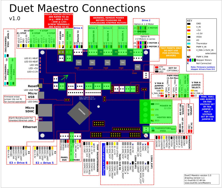
Full Wiring Diagram
Hardware Overview
What's in the box?
- Duet2 Wifi controller board v1.04b - for more information on PCB history
- USB A - USB Micro cable
- DIY cable connectors - build you own cable ends in case your motors don't connect
| List Price: | $ (with add-ons) | |
|---|---|---|
| Price: | $ (with add-ons) | |
| Sale Price: | $ (with add-ons) | |
| — Available for Pre-order — | ||
| Availability: | ... | |
| Est. In Stock: ... | ||
| Order Now: | Processed Immediately | Ships = 3500"> Free U. |
| Arrives after Christmas. Need something sooner? | ||
 S. Shipping
 This item cannot be shipped to a PO Box or APO/FPO/DPO address.
This item takes longer to ship due to its size and/or weight.
Qty
Checkout
Notify me when this is available
Duet3D Duet 3 6HC 3D Printer Controller Board
- Home
- Store
- 3D Printer Accessories
- 3D Printer Controller Boards
- TMC5160 Equipped Controller Boards
The Duet 3 6HC Mainboard is the heart of a fully-featured and expandible 3D printer control ecosystem. With support for up to six stepper motors, four temperature sensors, and ten PWM outputs, this 3D printer controller is a great choice for full DIY builds or as an upgrade to existing hardware. Ethernet connectivity means you can connect the printer to your local network for web-based control, calibration, and firmware updates. Duet 3D is hard at work developing expansion boards that will connect via the onboard CAN bus and continue to add value to this board into the future. If you are looking for a cutting-edge, fully-featured 3D printer controller, the Duet3 may be the board for you.
Remove from wishlist Add to wishlist loading...
Tagged: 3D Printer Controller Boards, 6+ Stepper Controller Boards and RepRap Firmware Controller Boards
Available Add-ons (2)
Show More Addons
Product No. M-1X8-786S
| List Price: | $255.00 |
|---|---|
| Price: | $255.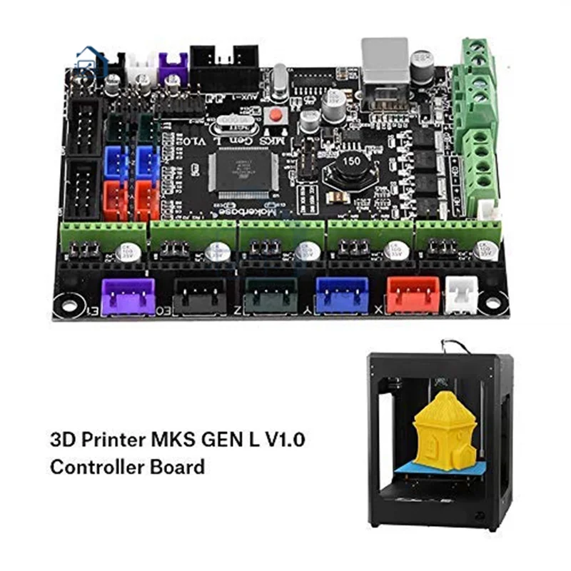 00 00 |
| Price: | $... |
| Order Now: | Ships calculating... Free U.S. Shipping |
Anytime you set out to upgrade the capabilities of your 3D printer, you have a specific goal in mind. Whether it be 32-Bit operation, the ability to add a second hotend, quieter motion control, or network connectivity, there are many great 3D printer features that don't come standard on each and every machine. The Duet3 6HC Mainboard supports everything listed here and more, making it a great choice for your upgrade build, no matter the base machine. Running RepRap firmware just like the other Duet boards before it, those familiar with the Duet3D family of products will be right at home with this mainboard.
Everything your 3D printer needs, all in one controller
Trinamic Stepper drivers with quality of life and functional capabilities for a top-of-the-line experienceThe Duet3 is built with Trinamic 5160 stepper driver boards built into the mainboard for seamless integration with your system.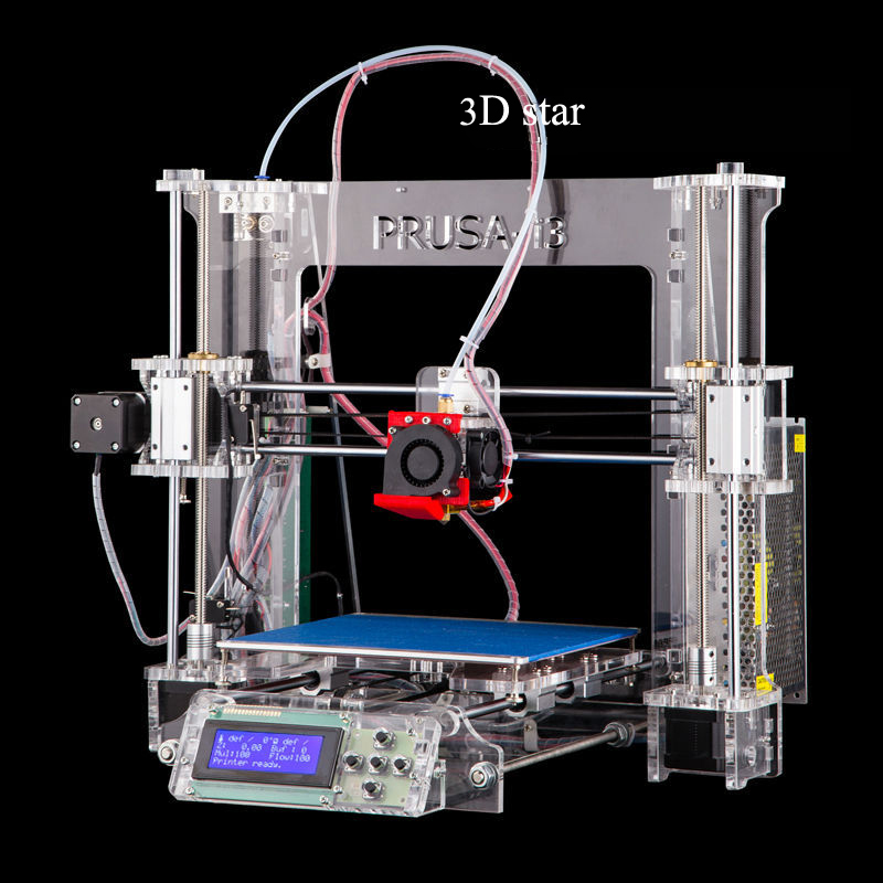 As the link between your Gcode and machine movement, stepper motor drivers are a very important aspect of any 3D printer or CNC machine. TMC5160's include the StallGuard 2 function for switch-less endstops, allowing your printer to simply butt up against the frame to have motion limits established. When this happens, the stepper drivers can detect a change in motor current, triggering the endstop. Also included is StealthChop2, one of our favorite Trinamic technologies here at MatterHackers. StealthChop2 creates virtually silent stepper motor movement, making your 3D printer quieter than ever before. Pair these driver boards with some stepper motor dampers and a well-lubricated axis for a 3D printer that you will have to watch to know it's even moving.
Powerful 32-bit process for smooth, high-quality operation
The Duet3 is built to be a premium experience today, but also to welcome continued expansion boards in the futureThe Duet3 mainboard is all about forward motion, learning, and growth.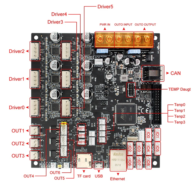 Out of the box, this mainboard has everything required for a premium experience with any 3D printer geometry but also includes expansion ability for future development as well. A dedicated high-speed bus for a single-board computer such as the Raspberry Pi opens up a new world of customization by leveling your 3D printer up into a full-on computer. Nine I/O headers for connecting endstop switches, probes, filament detectors, or any other sensors you can think of gives you the space for everything required today with room for future growth. Temperature sensor support is up to four thermistors or PT100's and in the event more connections are needed the onboard CAN bus is future-proofing at it's best. The Controller Area Network connection will allow for connection to Duet3 specific expansion and tool boards.
Ethernet connection as well as I/O and PWM outputs everywhere
Technical Specifications- Hardware Version: 1.01
- ARM Cortex M7 running at 300Mhz 32 bit processor
- 6 on-board TMC 5160 stepper driver boards
- StallGuard 2
- StealthChop 2
- 4.
 45A RMS & 6.3A Peak current
 - 256th Microstepping
- Dedicated SBC (Single Board Computer) connection
- 2 CAN busses for future Duet 3D expansion boards
- 10 PWM outputs
- 9 I/O ports
- 4 Temperature sensor inputs
- Thermistors or PT100's with the use of optional daughterboards
- Ethernet connectivity for network control
- Firmware: RepRap
- Duet 3 6HC MB
- SBC Ribbon Cable
- Custom connector parts - Build connectors to enable usage with any stepper motors
- Sticker - To display your pride in using a Duet 3 board.
Everything included with the Duet3
Printed circuit boards using a photopolymer 3D printer / Sudo Null IT News And in the last year or two, thanks to a strong reduction in cost, their photopolymer subspecies is also flourishing. Now such a printer is already available to almost everyone, and the number of their models on the market is multiplying every month.
Even when I just learned about the appearance of a new type of photopolymer printers a few years ago - in which the image of the layer for illumination is formed by an LCD, the thought flashed through me already then: "Hmm, what if we substitute a photoresist on a textolite?". But then it was a purely theoretical question - the prices for them were considerable, and the resolution and display area left much to be desired. However, today these printers can already boast of a decent resolution - from 30 microns per pixel, and a completely normal display area.
And as it turned out, with the help of an inexpensive modern photopolymer printer, it is quite possible to make boards with tracks / gaps from 0.15 mm.
I apologize in advance for such a voluminous graphomaniac, I myself did not expect that the note would get so fat...
I foresee the question "But why? In China, they will make normal boards with a mask and silk-screen printing for a penny!" I answer: now, most likely, there will be several iterations of finishing the board to a satisfactory state.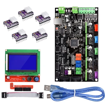 I made a board - tested it - made corrections. And so several times. Waiting every time for 2-3 weeks from China is not an option :) But when the final design of the board is determined - then, of course, normal production in China or on Rezonit.
Now let's get down to business.
Who does not know - here is a brief principle of operation of such a printer The main part of such a printer is an LCD display. Below this display is a 405 nm UV source. Above the display is a bath of photopolymer, which has a thin transparent FEP film as a bottom. A platform is lowered into the bath, on which the model is “grown”. At the beginning of printing, the platform lowers to the height of one layer from the film, the image of the first layer is displayed on the display, and UV illumination is turned on for a specified time. Illumination, getting through the "open" pixels of the display and the film onto the photopolymer, hardens it, so a hardened layer is obtained. The first layer sticks to the platform. Then the illumination is turned off, the platform rises to the height of the next layer, the image of this layer is displayed on the display, and the illumination is turned on. The second layer is cured by welding with the previous layer. And this is repeated over and over until the entire model is printed.
The idea to try to make a printed circuit board using such a printer came to me again about three years ago, when I bought myself an Anycubic Photon S printer. , then I just forgot about this idea, because and there was no need to make boards. But the other day, the need arose for the manufacture of several small boards, and with a high probability that as tests are made, changes will be made to these boards and it will be necessary to go through several iterations of "manufactured-checked-changed" in a short time. And the idea resurfaced.
To be honest, I thought that by now the Internet would be filled with the results of such experiments, the idea lies on the surface :) But to my surprise I found that the Internet is almost completely silent on this issue. There are separate notes, but there is no integrity and completeness in them. That's why I decided to publish this post - maybe it will help someone go all the way faster than me, and with less rakes :)
Well, the most important thing is that you don't need film and you don't have to struggle with increasing the contrast of the template. You also do not need a separate UV source with a place for its installation. And, of course, it is stylish, fashionable, youthful.
There are also disadvantages - the resolution of most modern 3D printers still does not cause much enthusiasm yet - the pixel size of all fluctuates around 0.05 mm. But this is already enough for confident manufacturing of boards with tracks from 0.2 mm and rather high chances of success with tracks from 0.15 mm. Due to the raster nature of such a template output, the position and size of elements on it can vary + -1 pixel, so I think it’s not even worth counting on tracks of 0.1 mm or less.
Let's go in order.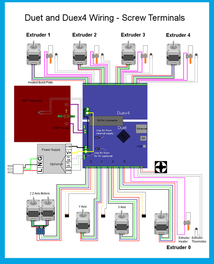
Task
It is necessary to make a printed circuit board at home using photoresist. Instead of templates and illumination lamps, use a photopolymer 3D printer that will serve both at the same time.
Let's divide the problem into separate steps-solutions for each moment.
-
Board development
-
Outputting layers in a printer-friendly format
-
Preparation of textolite with photoresist
-
Printer flare
-
Photoresist development, board etching
1. PCB development
Well, there are no questions. Whoever prefers to work in what program - in that one makes boards. The main thing is that the program should be able to display the result in some commonly used form. The easiest way I've come up with is outputting board layers to gerber files that can be fed to an online service. But you can also output to PDF or images.
2. Converting the CAD output to a printer friendly
This is where the trouble begins.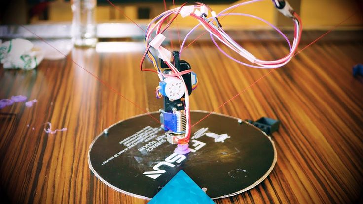 If almost all CADs can output to generally accepted formats - gerberas, DXF, printing to PDF, then 3D printer manufacturers so far categorically refuse to accept any file standard. Everyone is perverted as they can. The situation is largely saved by the fact that many manufacturers use motherboards from one Chinese company, Chitu Systems, in their printers. Thanks to this, many printers on such boards are able to understand one of the basic formats developed by the same company. And even often, if a file has some unique extension, then in fact it has the same basic format, just with a different extension. But it may differ in some details.
In any case, there is a free UVtools utility known among photopolymerists that can open files in one format and convert them to another format. It understands almost all formats on the market :)
I have tried two ways of preparing files with layers for the printer and I will describe both.
2.1 Gerber output and conversion to .
 photon
 The .photon file format is understood by the old Anycubic printers - Photon and Photon S. This is exactly the case when the printer manufacturer took the format from Chitu and changed its extension. In the original, this is the Chituvian .cbddlp format, so you can safely change the extensions of these file types among themselves and the printers will devour them like native ones.
Since I have a printer that understands this format, this method suited me perfectly. The limitations of this method are that the printer must understand .photon or .cbddlp files and have a standard display for most non-monochrome printers with a resolution of 2560x1440 and a diagonal of 5.5". manuals on how to do this for any CAD that can, in principle, mirror layers or not - it makes no difference, they can be mirrored in the utility during the conversion process.0003
Now open the online utility for converting gerber files - https://pcbprint.online/ and load the gerberas into it. By the way, this is a utility from a Russian developer who lives here.
It is easy to understand, although it does not contain any information or help. But here is a short guide:
For a single-sided boardUpload your gerbera in the main window with the "Upload file" button:
We made sure that everything is fine and the image meets expectations, if necessary, make a negative or mirror the image with the buttons in the top center, and press the button " Render layout":
Now press "Lauout" at the top right and get into another screen:
Here you first need to go to the settings (gear button at the top right) and there select the format of the output file "photon":
The time in "Exposition" can be left at default and change it to the desired one directly in the printer. But you can immediately put the right one if its value is already known :)
Close the settings and return to the previous screen. Here the output image is on a black space showing the working field of the printer. The image can be moved, aligned. When everything suits, we first press "Render", and when the "Download result" button next to it becomes active, we also press it. And save the proposed .photon file to a convenient location on your computer :)
For double-sided boards, things are a little more complicated due to the need to match them. Therefore, it is necessary to know very exactly the position of the image displayed on the printer's display in order to place the board on the display very accurately in accordance with it.
I had several options for solving this issue, but in the end I decided on the simplest of them, which did not require any mechanical conductors. To do this, I still in CAD in a separate layer (it is possible in the border layer or in any other "unnecessary" layer) I draw a frame around the board with a line of 0.15 mm and indented from the edges of the board by 0.25 mm. As a result, I get three gerberas - the top layer, the bottom layer and a separate empty frame.
I upload all three gerberas to the above site and then in a few steps I get three files for the printer.
Double-sided board in pcbprint.online/So, all three gerberas have been loaded. All of them are mixed together, but it's not scary:
Now hide the top and bottom layers, leaving only the frame (by clicking on the eyes in the names of the gerberas).
Click "Render layout" and go to the "Layout" screen with the button in the upper right corner. We see an empty frame, drag it to the desired position on the black field of the display, click "Render" and "Download". The first file for the printer is ready.
Switch back to the gerber screen with the "PCB comose" button. Redisplay the first layer (the frame layer still remains visible), mirror if necessary, and click "Render layout" again. Again we go to the output screen and now there are two pictures hanging on the display field - a separate frame and the first layer with a frame. The frame remained in the same place where we pulled it last time.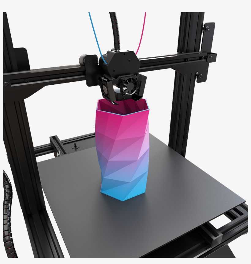 And now our task is to exactly combine the frame of the first layer and the empty frame:
Click "Increase" and combine in one of the corners. In this case, in no case should you move the empty frame that we set in the last step!
Combined, click "Render" and "Download", and we have a second file for the printer. Before returning to the gerbera screen, we delete the render layer with the frame, we should again have an empty frame. And now we return to the gerberas, hide the first layer and display the second one, look at the need to mirror, click "Render layout" and go to this screen again. In the same way, we combine the layer frame with an empty frame (which cannot be moved!), then "Render" and "Download".
Everything, all three necessary files for the printer are ready.
All this hemorrhoids allows you to generate for the printer files of an empty frame and layers with a frame in the same place on the printer display with high accuracy. The empty frame serves to aim the board, more on that below.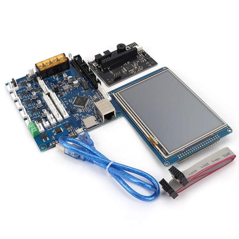
If necessary, the resulting .photon files can be converted to the desired format using UVtools :)
2.2 Output layers to PDF or images
The second method is perhaps more confusing, but its great advantage is versatility, it is suitable for any printers, whose formats are supported by UVtools. I will describe it only in general terms, because. There are quite a lot of tools and specific ways to implement it, and everyone can choose them according to their preferences.
So, the goal of the first step is to get a picture with a size equal to the resolution of the printer's display, preferably in a lossless compression format. In this case, the image of the layer in the picture must correspond to the real size in the scale of the display.
If CAD allows you to output directly to the picture - great, output to it. If the resolution of the output image is configurable - specify the resolution of the printer display. It is elementary to calculate it - we divide the number of pixels across the width of the display by the width of the working area in mm and multiply the result by 25. 4, we get the resolution in pixels per inch. If the resolution is not set, then set the image size as large as possible so that there are at least 15-20 pixels per 1 mm of the board.
If output to image in CAD is not available, then output to PDF. This PDF will need to be opened in another program and converted to an image. Photoshop, Corel, maybe other programs can do this... The requirements for image resolution are the same. For example, in Photoshop, when importing a PDF, you can immediately specify with what resolution to convert to an image. For example, for common displays with a resolution of 2560x1440 and a diagonal of 5.5 "the resolution is approximately 537.566 PPI (pixel size - 0.04725 mm).
The resulting image will need to be changed in some image editor, bringing its size to the resolution of the printer's display. In this case, the layer image must be scaled to the real one (taking into account the pixel size of the printer display) or saved without scaling if the PPI of the display was specified when importing the image.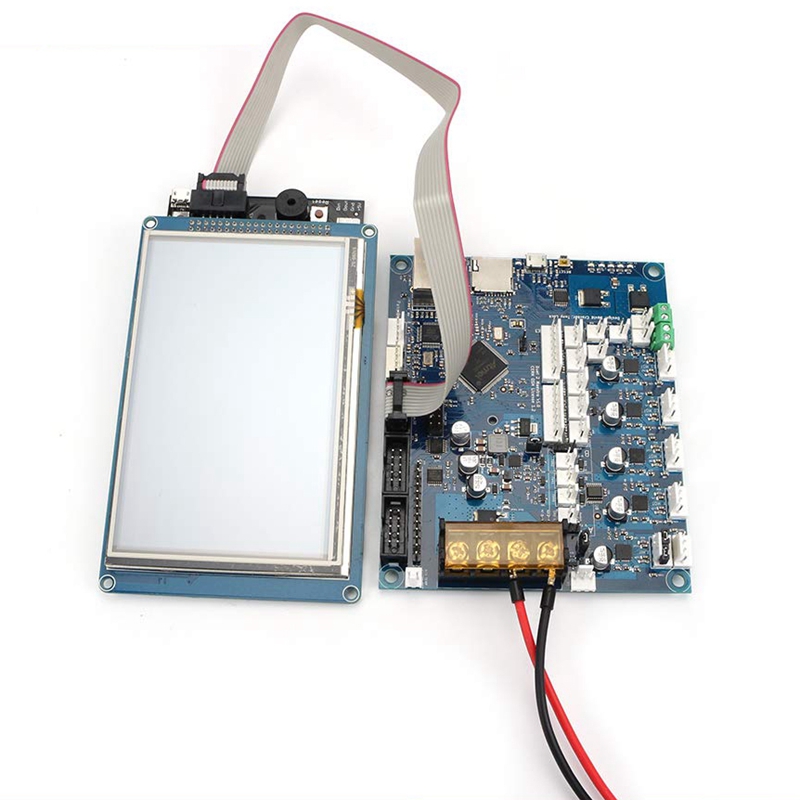
UPD: in the comments @0x3f00 gave a link to his converter of PNG images to files for the .photon printer - https://github.com/0x3f00/PhotonCpp/releases/tag/v1.0.0 . There is also an instruction for using it just for the purpose of manufacturing boards - https://github.com/borelg/PhotonPCB.
2.3 There is another way, but it is very resource-intensive
You can output layers to PDF, then open this PDF in Corel, convert it, save it in DXF, extract a three-dimensional object from this DXF, which you can push into the printer's slicer.
Necessary transformations in the vector editor:
-
Connect all curves.
-
Convert outlines to objects.
-
Merge intersecting objects.
You can extract a three-dimensional object from DXF, for example, SolidWorks. Fusion360 also seems to be able to. Who else is capable of this - I honestly don't know, but in theory any CAD that can import DXF as a sketch.
Thus, for example, I made a model for determining the exposure time of the photoresist.
3. Preparation of textolite with photoresist
The Internet is simply littered with articles on this topic, but for the sake of integrity and for the sake of some specific points, I will also describe such well-known stages as the preparation and etching of textolite.
My first experience with such a fabrication was a couple of days ago with a domestic photoresist PF-VShch. Taking into account the last yesterday's experience, I categorically advise not to waste time on this photoresist, but immediately take a decent one - Ordyl Alpha 350(330) :) They say that Kolon is also decent, but I have not tried it. With Ordyl photoresist, the results are much more stable and accurate, it is easier to develop and adheres much better to the foil. And he can forgive those mistakes that will be critical for the PF-VSC. And what is important - it is sold in a bunch of places quite inexpensively.
3.1 Preparing the textolite
To begin with, the textolite should be smooth, very preferably with a smooth foil without scratches or dents. Otherwise, the chances of success are reduced.
If a double-sided board is being made, then you need to immediately cut the board out of the PCB exactly to size. If there is any CNC router, then you can drill all the holes and cut along the contour in one installation, as I do. If not, then it is better to leave the drilling for later, when the board is etched.
After this, the textolite blank must be very carefully cleaned and degreased. This can be done with a kitchen abrasive sponge (but not used for washing dishes on which fats have already accumulated) and a scouring powder like Pemolux. Very carefully, slowly three every square millimeter of foil, without touching it with your fingers. In general, I categorically do not advise touching the foil with your fingers after the start of cleaning, there should not be the slightest even the faintest greasy spot on it. After cleaning, rinse thoroughly in running water, shake off excess water and allow to dry. I do not advise blotting or wiping with anything, because.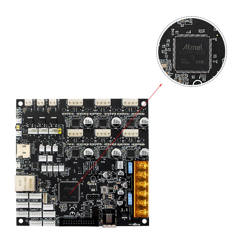 grease can be applied, even from a new napkin.
3.2 Application of photoresist
Also a fairly common topic on the Internet, so I'll go over it briefly.
Photoresist usually comes in sheets or rolls. It consists of three layers - two protective films and the photoresist itself between them. A piece is cut off from the photoresist according to the size of the board + 5 mm in length and width, then a matte (polyethylene) protective film is removed from it.
the second, glossy (lavsan) must remain on it until the etching stage.
The easiest way to remove the film is with a piece of tape. It is glued with its edge to the corner of the photoresist and then folded back, pulling the protective film along with it.
After removing the matt film, the photoresist is applied to the edge of the board and smoothed along this edge with a finger. The rest of the photoresist is supported by weight, without tension, but in such a way that as little as possible of its area lies on the foil.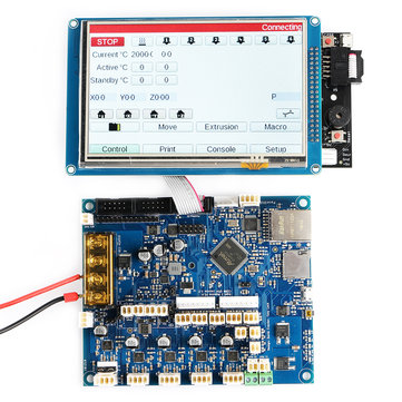
Please note that if the Ordyl photoresist falls on a well-prepared textolite, then it can firmly stick to it, and without bubbles it can no longer be rolled. You have to scrape it off and do it all over again. And PF-VShch can fall as much as you like - it definitely won't stick :)
Now the knurling itself. If you have a laminator, in which the textolite will crawl through the thickness, then it's just wonderful. We make an envelope-type strip of paper folded in half, put a textolite with a sticky edge of the photoresist in it, and serve this sandwich into a laminator heated to 100-110 degrees. At the same time, we continue to hold the photoresist so that it comes into contact with the textolite foil only directly at the inlet of the laminator.
That's all for Ordyl, for PF-VShch it will be harmless to roll a couple more times.
If there is no laminator, then smooth the photoresist to the textolite with your finger from edge to edge, gradually lowering it onto the textolite. The main thing is not to catch the bubbles. After all the photoresist lay on the foil, we take a hair dryer and heat the textolite to 70 degrees, after which we iron the entire photoresist once again.
After knurling, let the textolite with photoresist lie down for 15-20 minutes, or at least until they cool down to room temperature - according to the recommendation of the photoresist manufacturer.
And now everything is ready to highlight the layer pattern :)
4. Printer highlights
I want to warn you right away: looking directly into the glowing display of a photopolymer printer may not be very good for the eyes. Although not true UV (405 nm), the brightness is quite noticeable and can be harmful to the eyes. Therefore, I recommend using colored or tinted goggles. I think even sunscreen will do.
First, you need to remove the bath and platform from the printer, they are completely unnecessary for this business and even interfere. This completes the preparation of the printer :)
Lighting also has different options. If you have a one-sided board and the blank is larger than the size required for the board, then everything is simple - throw the file obtained at the preparation stage into the printer and, knowing the approximate place for displaying the image on the display, put a textolite with photoresist in this place. Then start printing the file and wait until it is completed. Everything, the photoresist is exposed, it is possible to develop.
If the workpiece is equal in size to the board being made and the error with the position of the workpiece on the display is unacceptable, then in this case it is necessary to remove the frame during preparation, as is the case for a double-sided board. Illumination also occurs using a frame, similar to a double-sided board, only without the second side and the second layer.
So, the illumination of the double-sided board. We throw all three files into the printer - with a frame, with the first layer and with the second layer. We put the workpiece next to the printer in quick accessibility. If it is already pre-drilled, it will be useful to make sure that it lies in the correct position so that you can quickly take it and immediately put it on the display. To do this, we run a file with a layer planned for exposure, and compare the layer pattern on the display and the orientation of the board next to the printer.
Printing a file with one frame. As soon as the frame lights up on the printer display, we take the workpiece and put it approximately inside the frame. While the frame is being illuminated, we align the workpiece so that it is exactly in the frame, with the same indentation of the frame from the edges of the workpiece on all sides.
In the photo, I gave an example with a ready-made board, because I did not take pictures during the manufacturing process. Well, reflections interfere quite strongly, alas... But I think it's understandable :)
That's it, the position of the workpiece is verified, printing of the frame file can be interrupted or wait for it to finish.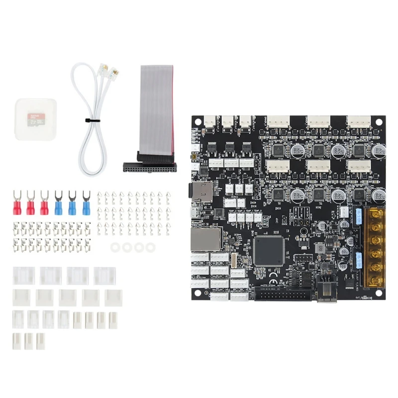 Without moving the workpiece, run the file with the first layer and wait for it to finish. We illuminate the second layer (the second side) in the same way - we launch the frame, place and align the workpiece, without moving it, we launch the second layer. Before this, just in case, you can make sure that the workpiece will lie in the correct orientation, as before the first layer.
If the workpiece is not completely flat and does not fit the entire area of the display, then you can press it down from above with some heavy flat piece of iron. You just need to make sure that this piece of iron does not interfere with the platform lever, which will go down with the start of printing - the printer thinks that this is a normal photopolymer print and you need to lower the platform to the bottom of the bath :)
Illumination time can be different from printer to printer . It depends on the power of the emitter, and on the optical illumination system, and on what type of display is worth - monochrome or RGB. Here already it is necessary to select each individually. For orientation, I can say that I got the best result with the Ordyl photoresist at an exposure time of about 90-110 seconds. With photoresist PF-VShch - about 10-13 minutes. Printer with paraled, illumination power slightly less than 50 watts.
After exposure, the workpiece should be allowed to rest for 15 minutes - this is according to the recommendation of the photoresist manufacturer. Ordyl changes the color of the highlights quite noticeably, so it's pretty easy to control the highlights. Unfortunately, the photo did not convey it well, it can be seen better with the eyes.
5. Development, etching
Everything here is according to the recommendation of the photoresist manufacturer and according to the classics of the Internet.
All necessary chemicals were purchased inexpensively from Auchan. Even hydrogen peroxide 6% - this was a surprise for me, I had never seen it in hypermarkets before, and even in liter bottles.
For one session you need:
-
Soda ash - 1.5 grams
-
Hydrogen peroxide - 150 ml for 3% (or 75 ml for 6% + 75 ml of water)
- citric acid
-
Salt - 7.5 grams
-
Alkali (caustic soda, sodium hydroxide) 5-7% - 100 ml
With the cheapness and ease of buying all the components around the corner, I am in favor of preparing a new solution for each board. Although the etching solution, as they say, is not stored anyway. A solution of soda ash noticeably "poorer" in the process of development. Unless caustic soda can be reused, but is it worth it to keep another bottle ...
Both Ordyl and PF-VSH appear in a weak solution of soda ash. For PF-VShch - 1-2%, for Ordyl - 0.8-1.2%. For Ordyl, we take 150 ml of water and dilute 1.5 grams of soda in it. The solution can be heated up to 30 degrees, this will speed up the development, but it is important not to overdo it, otherwise the illuminated areas may begin to be damaged.
Ordyl appears rather quickly. Already after 10-15 seconds, the illuminated pattern begins to become more and more contrasty, the unexposed areas gradually dissolve, become thinner and become paler.
To speed up the process, it is recommended to shake the bath so that the reaction products are washed off the surface of the workpiece. For this I adapted my old 3D printer, its table and shook and heated the bath with the solution during development and etching :) Two minutes passed before there were at least some signs that development had begun. In addition, if Ordyl does dissolve, then PF-VShch first swelled like gelatin and discolored, and only then began to slowly dissolve.
At the end of development, you can go over the boards with a hard paintbrush (or soft toothbrush) several times in different directions to help flush out any remaining photoresist from tight spots. Ordyl holds on tight, this procedure should not disrupt it, but with PF-VShch you need to be very gentle, even without a brush it strives to exfoliate on thin paths.
After etching, the workpiece must be rinsed in cold water so that the soda residues do not continue to attack the photoresist and so as not to clog the etching solution with them.
The result should be something like this, maybe even better :)
More detailsScale of the grid square - 0.2 mm:
The scale is the same. Here you can see the raster component of the illumination, the pixels stick out:
Etching was also done according to the traditional recipe, popular on the net:
It is better to heat the solution to 40-50 degrees, then the etching goes much faster. This is my first experience with this solution. I used to poison with ammonium perchlorate, and even earlier - with classic ferric chloride. To be honest, I can't really express how I feel about this solution. On the one hand, it poisons rather quickly, is transparent, does not get dirty, and is relatively safe. On the other hand, it seemed to me that it was easing quite a lot ... But maybe it just seemed, I haven’t been making boards for 10 years and I forgot how it all worked when the trees were big :)
After etching, the exposed photoresist must be removed from the workpiece, and this is done in caustic soda.
 On my bottle of cleaner it says "at least 5% but not more than 15%" and it takes 5-8% to remove the photoresist. I diluted the product 1:1 with water and this solution did the job perfectly. The photoresist does not dissolve in it, it simply peels off the foil after 2-3 minutes and begins to float in tatters in the solution.
 After that, the board is thoroughly rinsed under the tap and... The board is ready!
Summary of my experience
Overall I am satisfied. I did not expect to get tracks / gaps of 0.1 mm and I did not get them. Here, the capabilities of the printer are severely limited (pixel size), and in general, good experience is needed for such results. But I was hoping to get at least 0.2 mm, and if I'm lucky, then 0.15 mm - and I got it. 0.2 mm confidently, 0.15 mm - well, so-so... If you try, you can achieve :)
There were some flaws - it was not pickled in some areas, and imperfect alignment of layers and holes. But neither is critical. As for the non-mordant - I think that I just hurried to take it out of the developer, I was afraid after PF-VShch that thin paths would begin to peel off.
 Although in the reviews people write that it is quite difficult to re-develop this Ordyl, you need to try for this. Imperfect alignment of layers and holes is to be expected. From such a simple method of alignment, I expected an error of 0.1-0.2 mm, which I got, but it suits me.
 Thank you for reading.
And finally, a few photos of my results. Exposure time test, from 1 to 2 minutes. You can see the pads displaced relative to the holes. Printer. Alternative to LUT.In general, I have been doing all sorts of electronic crafts for quite some time, and I decided to purchase a 3D printer, so to speak, for my hobbies, one of my hobbies is, as it is written on top of electronics. And where in electronics without breadboards, textolite and breeding tracks. In general, I decided to whip up a stray, so that I could quickly make printed circuit boards without any 'perturbations'.
Of course, I initially got into the Internet, because why reinvent the wheel.
 I found a couple of articles on this topic, and a lot of options for lasers. But I didn’t have a laser, firstly, at hand, but there was a hunt, two days after buying a 3D printer, to create. Well, after seeing what others are doing, I decided to simply simply delete the layer around the tracks. than in the form of a 'needle'.
 Step 1
Well, in general, there were thoughts, but the hands 'went' to do, first a 3D model of the casing was modeled, in which the same needle would be located.
[IMG ID=205201 WIDTH=339 HEIGHT=450]
Scraper housing model.
Step 2
The scraper that would remove the water-resistant coating from the PCB was made from a 3mm guide from the SD drive. At the end it is sharpened so that the edge is sharp. It was also necessary to figure out how to dampen this scraper so that it had an upward stroke when pressed against the textolite. To do this, the piezo lighter was disassembled, and a donor in the form of a spring was taken from the piezoelectric element, which served as a damper for the needle.
[IMG ID=205202 WIDTH=451 HEIGHT=337]
The same damper in a 3mm hole.
[IMG ID=205203 WIDTH=449 HEIGHT=336]
All necessary scraper materials. (Ruler for scale)
[IMG ID=205200 WIDTH=337 HEIGHT=450]
Final result.
After the casing was printed out, the remains of the substrate were cut off, the hole was lubricated with silicone, for easier sliding of the needle, a spring was inserted into the hole and a needle was inserted at the end. Which, with the help of a spring, can damp up to 5 millimeters vertically. Due to the high casing, the needle does not play in it at all to the touch and to the eye, which will help minimize inaccuracies in drawing a pattern on the textolite.
Step 2.1
We put the scraper in place, using elongated studs, the length of which was 5 cm (bottom), the upper bolts are screwed directly to the cooler. In general, it turns out that the whole structure is held on studs that are screwed to a stepper motor, which supplies the filament to the extruder.
 The end result looks like the pictures below.
 [IMG ID=205219 WIDTH=337 HEIGHT=450][IMG ID=205218 WIDTH=337 HEIGHT=449]
Step 2.2
We set the dead point along the Z coordinates so that our scraper does not accidentally scratch the table, and so that the extruder nozzle does not touch the textolite. To do this, a 3-4 mm plug was put on the Z-axis limit switch so that the nozzle would not touch the textolite. It is also clear that the length of the needle will be different for everyone, and everyone will need to measure it out on their own. As an option, you can unfold everything, screw a spring, a toothpick into the hole, and at the same time, simply cut it off a little bit, choosing the length of the needle that suits you. Then, having determined the length that is suitable for you, saw off part of the guide and sharpen it on one side.
step 3
I don't know about CNC as well. But with the help of a search, I found a program in which you can make Gcode, for passing certain coordinates, in order to ultimately get the desired PCB pattern on PCB and a program in which you could print Gcode.
 These programs are FlatCam and Pronterface.
 Step 4
Trying to understand FlatCam for my needs took a couple of hours of my life. But in the end, I figured out how to work with it. For this program, we need to export our board in Gerber format. To do this, in the Sprint layout, click File - Export - Gerber format. And select the layer that we need. Also in Sprint, when creating a new board, the coordinates go not from 0/0 but from 0/100 as you can see in the picture, for zero coordinates, you will need to make the board width 100mm, and lower your board down to zero coordinates , otherwise in FlatCam the image will be shifted up.
[IMG ID=205204 WIDTH=750 HEIGHT=436]
Then open the FlatCam program. Click File-Open Gerber, and select our newly exported file.
[IMG ID=205205 WIDTH=750 HEIGHT=406]
We see the picture (pay attention to the coordinates, which I mentioned above, when exporting from Sprint Layout), which we exported, select your board in the Project column, and click adjacent Selected button.
[IMG ID=205214 WIDTH=750 HEIGHT=406]
We see your drawing and adjust the settings. What the settings mean, we see in the picture. At the end of the settings, click Generate Geometry.
[IMG ID=205213 WIDTH=750 HEIGHT=406]
In the projects column, select the newly appeared project, and click Selected again.
[IMG ID=205215 WIDTH=750 HEIGHT=406]
Here we also set the settings you need, and click the Geometry button.
[IMG ID=205216 WIDTH=750 HEIGHT=406]
Again, a new project will appear in the Projects column, and from it we finally export our code by pressing the Export G-Code button.
Step 5
We take textolite and fasten it with stationery clothespins to the printer table.
[IMG ID=205221 WIDTH=374 HEIGHT=499]
At the same time, we immediately set the appropriate position of the textolite along the zero points of the X/Y axes.
Step 6
Open our saved G-Code in Pronterface, connect it to the printer and the only thing left is to attach the scraper, and set zero points.
 to do this, on the left side, press the white button of the house, your needle goes to its 'Home position', and here again you can see if your textolite is right, if not, you can align it.
 [IMG ID=205220 WIDTH=600 HEIGHT=426]
Then, using the same program, you can set the ideal needle position for you by selecting the Z height, in which it removes a layer of waterproof material well (in my case, a waterproof marker) . when you have found the ideal position, when the needle touches the textolite and removes the marker well, then you need to take and write down this value in order to use it in FlatCam for the cutting height. Then we slowly raise the needle up along the Z axis and look when it stops touching the textolite, and throw another couple of tenths of a mm so that the needle does not touch the textolite when moving between the coordinates of the picture. We also use this value to set up G-CODE in FlatCam.
And finally, when you have found all your ideal positions, take the already made G-CODE, Open it with Pronterface, and print your board.
Learn more