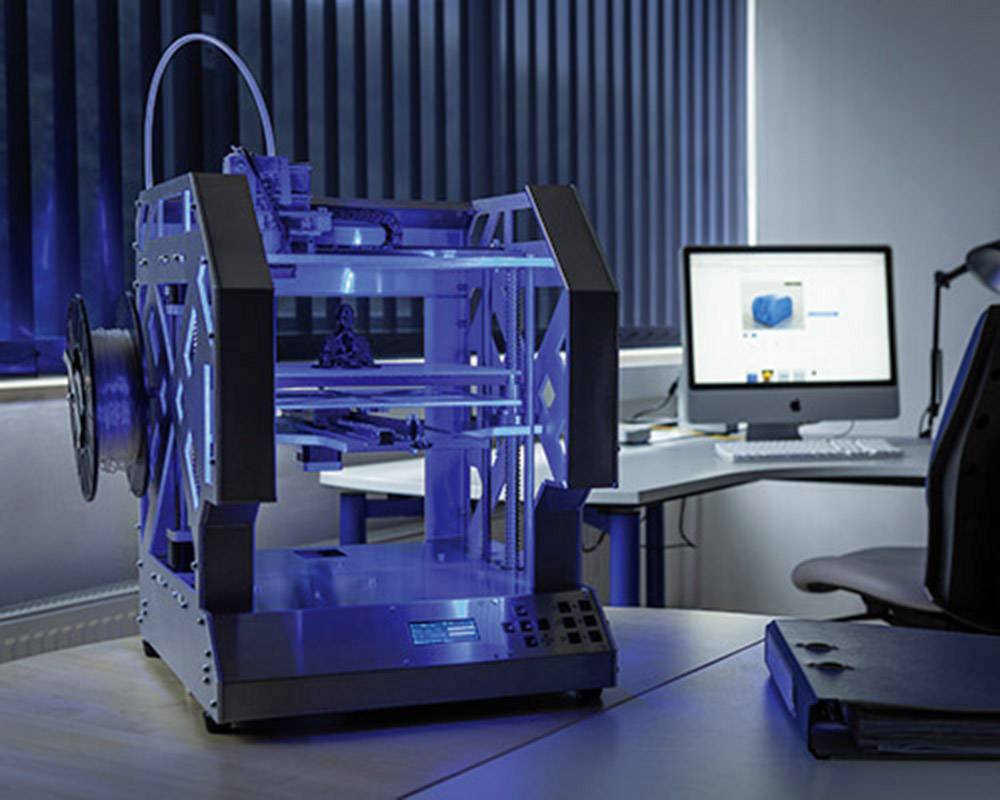
3D printing semiconductors
What's Possible Now and in the Future?
Ziv Cohen
Application Manager, Nano Dimension
The semiconductor industry gets a lot of attention—and for good reason. Integrated circuits make technology possible, and these devices are built on the back of semiconductors.
Semiconductor manufacturing processes have come a long way since Robert Noyce invented the integrated circuit in 1959. With the rise of Industry 4.0 and the wide array of additive manufacturing processes, one naturally wonders whether the electronics industry will advance to 3D printing integrated circuits at full scale.
In this discussion, the question naturally arises: Why use additive manufacturing processes to produce integrated circuits? 3D printing is already being used to produce fully-functional PCBs with unique geometry, interconnect architecture, and various levels of component embedding. The ability to 3D print integrated circuits and other semiconductor devices directly into a PCB allows low-volume fabrication of highly specialized devices with unique form factor and capabilities.
IC dies on a silicon wafer
The Current State of 3D Printing Integrated Circuits
Silicon, III-V, and II-VI semiconductor manufacturing processes are highly advanced and are used to produce integrated circuits with less than 10 nm gate sizes. Currently, the most advanced 3D printing processes provide near micron-level resolution and co-deposition of multiple materials.
Co-deposition is critical for 3D printing integrated circuits because conductors and semiconducting materials must be printed simultaneously. The resolution of the most advanced 3D printing systems must still improve before VLSI is possible. In addition to improving device performance, miniaturization will provide much lower power consumption for switching logic gates.
As an example of what is currently possible with 3D printing integrated circuits, researchers at the Air Force Research Laboratory and American Semiconductor recently 3D printed microcontroller SoCs from polymers on a flexible silicon substrate. These microcontroller units offer 7000x memory compared to other flexible integrated circuits at the time. Some envisioned applications include environmental or strain sensing, as well as munitions inventory monitoring.
A flexible microcontroller integrated circuit. This circuit was fabricated using polymers on silicon.
Currently, thin-film transistors (TFTs), diodes, LEDs, can be 3D printed from organic polymers with commercially available and experimental systems. The 3D-printed TFTs can have various contact/gate configurations and can easily be scaled horizontally and vertically. Polymers can be easily doped and functionalized, allowing their electronic and optical properties to be tuned to meet the demands of different devices.
Using polymers on a semiconductor wafer is a natural route to pursue 3D printing integrated circuits. Electrical contacts can already be deposited in an additive manner through a mask (i.e., thermal evaporation, PVD, or CVD), followed by deposition of semiconducting polymers and larger conductive tracks with a 3D printer. Their adaptability to low-temperature processes also makes them ideal for 3D printing integrated circuits directly on standard semiconductor wafers.
Other researchers are working on advancing additive manufacturing processes and materials to enable 3D printing integrated circuits. As an example, the University of Hamburg and Deutsches Elektronen-Synchrotron developed a 3D printing process that can enable the fabrication of integrated circuits. This process uses a mesh of ~20 nm silver nanowires as conductive elements and a thin film of polymer as an insulator or semiconducting material. This process is still in the research phase, but it illustrates how unique nanostructures can be used to fabricate semiconductor devices that rival silicon integrated circuits.
The Economics of 3D Printing Integrated Circuits
In any manufacturing process, the cost structure involved in manufacturing is an important driver of the price of a finished device. Integrated circuits succeed or fail based on the cost of the die on the wafer—when more dies can be placed on a single wafer, the costs per device decreases. The cost structure of integrated circuit manufacturing is responsible for the high costs of highly specialized, low-volume integrated circuits. An excellent example can be found in the defense industry, where the cost of a single FPGA for a complex system can reach tens of thousands of dollars.
The unique cost structure of 3D printed devices changes this economic dynamic. 3D printed integrated circuits do not need to be produced on a wafer and can even be manufactured individually. Because 3D printed devices can be produced with predictable fabrication time, and the cost structure is complexity agnostic, the costs involved in 3D printing electronics depends on the weight of the materials used. This makes 3D-printed integrated circuits highly cost competitive for low-volume production compared to devices produced on semiconductor wafers with standard processes.
Challenges in 3D Printing Integrated Circuits
Commercially available printers are becoming more advanced, and the range of materials useful with these systems is expanding. That being said, there are still some challenges in 3D printing integrated circuits with the same level of performance as integrated circuits on monolithic circuits. These challenges involve finding rigid semiconducting materials that can be adapted to a standard 3D printing process, optimizing these materials for different frequency bands, and bringing printing resolution closer to the nanometer level.
A lithographic process may aid in 3D printing integrated circuits with less than one-micron resolution.
The fact losses and parasitics can be optimized in a variety of polymers for specific frequency bands allows these materials to compete with GaN, which is currently the best option for fabricating RF integrated circuits and SoCs. GaN is currently used in the best SoCs for high-frequency radar modules, as well as in power amplifiers for microwave and mmWave signal chains. Polymers are already used to 3D print substrates for building flexible and nonplanar PCBs, so it is natural to extend these materials to integrated circuits and other semiconductor devices.
To increase the printing resolution, the additive manufacturing industry may need to devise a completely new printing process. Currently, inkjet 3D printing provides among the highest resolution features for 3D printing PCBs, but it remains to be seen if this process can be improved to provide resolution less than 1 micron.The future of 3D printing integrated circuits will likely adapt a photolithography process or functional self-assembly process to produce integrated circuits with competitive resolution.
Innovative companies that are interested in 3D printing integrated circuits and fully-functional PCBs need an additive manufacturing system designed for full-scale production of complex electronics. The DragonFly LDM system from Nano Dimension is ideal for in-house full-scale PCB fabrication of complex electronics with a planar or non-planar architecture. Designers can embed standard components and can experiment with 3D-printed integrated circuits.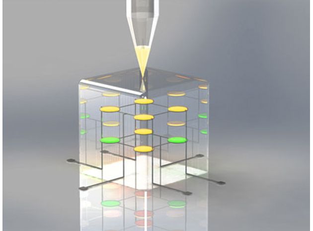 Read a case study or contact us today to learn more about the DragonFly LDM system.
3d printing | 3D printing applications
Ziv Cohen
Application Manager, Nano Dimension
Ziv Cohen has both an MBA and a bachelor’s degree in physics and engineering from Ben Gurion University, as well as more than 20 years of experience in increasingly responsible roles within R&D. In his latest position, he was part of Mantis Vision team—offering advanced 3D Content Capture and Sharing technologies for 3D platforms. The experience that he brings with him is extensive and varied in fields such as satellites, 3D, electronic engineering, and cellular communications. As our Application Manager, he’ll be ensuring the objectives of our customers and creating new technology to prototype and manufacture your PCBs.
How 3D Printing Is Disrupting The $439 Billion Semiconductor Industry? - Asia Pacific Metalworking Equipment News | Manufacturing | Automation
Is 3D printing a solution to enhance supply chain resilience for such a core component of the modern tech world?
BY LAURA GRIFFITHS
Conventional semiconductor manufacturing processes limit designers in terms of interconnect architecture, planarity, and substrate shape. In contrast, 3D printed circuit boards are not limited by subtractive manufacturing limitations, saving semiconductor companies a lot of time, effort, and money, and providing designers with increased freedom to design circuit boards with sophisticated architecture and customised designs as required.
Working with a system that is designed for 3D printing circuit boards is an excellent way to complement an existing semiconductor manufacturing process for low-volume, high-complexity boards. The layer-by-layer printing process allows low-volume manufacturing runs of boards with the desired level of complexity, including non-planar circuit boards and high-value boards with very complex shapes.
Why 3D Print Components?
Wafer table thermal management
Better thermal management of critical semiconductor equipment components, such as wafer tables, can improve semiconductor equipment accuracy by 1–2 nm and simultaneously improve speed and throughput. An increased machine speed and uptime leads to more wafers processed and higher overall lifecycle value.
During lithography, keeping temperatures within milliKelvin (mK) ranges is critical as any system disturbance has an impact. Through design for additive manufacturing (DfAM), it’s possible to optimise internal cooling channels and surface patterns, thus dramatically improving surface temperatures and thermal gradients while reducing time constants. A large semiconductor capital equipment manufacturer using AM to produce their wafer tables realised an 83% decrease in ΔT (13.8 to 2.3 mK), and a 5-time reduction in time to wafer stabilisation.
Another benefit of using AM to produce wafer tables is structural optimisation and tables with reduced part counts and assemblies. Producing parts using traditional technologies relies on brazing to join parts together, which is a lengthy, low-yield process with a 50% rejection rate. Replacing multipart assemblies with monolithic additively manufactured parts increases reliability, improves manufacturing yield and reduces labor costs.
Semiconductor wafer table thermal management – 3D Systems
Manifold fluid flow optimisation
Using traditional manufacturing processes to produce complex fluid manifolds results in large, heavy parts that have non-optimal fluid flow due to abrupt transitions between components, and channels with sharp angles that lead to disturbance, pressure drops, stagnant zones and leakage.
When AM is employed to produce these same manifolds, engineers can optimise their designs to reduce pressure drop, mechanical disturbances and vibration. A 90% reduction in flow-induced disturbance forces reduces system vibration and realises a 1–2 nm accuracy improvement.
Structural optimisation and advanced flexures
AM gives designers the flexibility to optimise the structural topology of your part (i.e. lightweighting) with a suite of high-strength metal alloys. These designs can more precisely meet the performance requirements of semiconductor capital equipment, improve the strength-to-weight ratio and deliver a faster time to market. Lightweighting semiconductor components and advanced motion mechanisms reduces inertia and improves lithography and wafer processing machine speed and uptime, leading to more wafers processed. In one example, a semiconductor capital equipment manufacturer was able to employ AM to achieve greater than 50% weight reduction in flexures, 23% higher resonant frequency and reduced system vibration.
A likely scenario is that AM will significantly enable newer machines that are either shipping today or will be shipping in the next 1-2 years. With this runway, there is ample time for component and system level redesigns, which will increase productivity and quality. Additionally, the manufacturers will still have enough control over those systems to rigorously test and prove performance gains.
However, while opportunities are indeed emerging, it’s not necessarily a new market for additive nor 3D Systems. At the 3D printing pioneer’s Leuven office in Belgium, major semiconductor equipment manufacturers are said to have been leveraging its direct metal printing for well over a decade. What began as a “secret metal printer” used to print parts as a service has matured to what Scott Green, Principal Solutions Leader at 3D Systems described as “a couple of hundred” successful production projects.
“There’s maybe ten areas in semiconductor capital equipment where we’re contributing regularly,” says Green, citing opportunities in lithography, wafer handling and metrology. Green also pointed to examples of recent large-format EUV (Extreme ultraviolet lithography) machines which can contain well over 100,000 parts.
“The needs and challenges of the semiconductor fabrication industry today are directly aligned with what a direct metal solution offers,” Green tells TCT magazine. “They have challenges where, in order to really push the limits of physics, you’ve got to totally eliminate uncertainty and noise inside of a system and really optimise all the parts of handling, cooling, fluid distribution, light collimation. It’s a very complex machine.”
The design freedoms and part consolidation afforded by additive could offer a solution for parts like heat exchangers, gas manifolds and nozzles. Instead of having tens of components vibrating against each other in an assembly, you could potentially reduce the number of moving parts and links in your supply chain down to one.
VELO3D is working in collaboration with Lam Research Corp to develop new 3D printing materials and applications for the semiconductor space. (Image credit: VELO3D)
The Challenges of AM Adoption Moving Forward
3D printing electronic components is not without its hangups, however. In an interview with TCT Magazine, VELO3D CEO Benny Buller explains that AM is best used for replacing existing parts—not redesigning a system altogether.
“When you are doing legacy parts that you are already producing in one way and just want an identical replacement by additive, the barrier for qualification is much lower,” he said. “But when you start having to redesign the system or the assembly so that you can manufacture, well that’s not fine, because now you’re driving yourself into a lot of risk.”
Buller also notes that AM struggles to deliver the cleanliness and surface control one would find in the cleanroom of a traditional fab. At each layer of the semiconductor fabrication process, wafers are expected to be free of particles that are nanometers in size. This attention-to-detail cannot be replicated in an at-home or in-office 3D-printing environment.
When dealing with the precise chemistries, gases and temperatures expected by the semiconductor industry, those risks simply cannot be afforded. Those same complexities, however, Buller believes suit the capabilities of additive well.
“These are the classical problems additive manufacturing is really good at,” Buller explains. “Control of heat, control of flow, whether it’s flow in gases, form of chemicals, whether it’s forming liquid flow, these are the places where additive manufacturing is really powerful.”
One crucial area where AM does present a challenge, however, is cleanliness, a field Buller is familiar with having spent the early years of his career on the inspection side of the semiconductor space.
“Additive manufacturing, compared to some other manufacturing technologies, has struggled delivering this level of surface cleanliness and this level of surface control,” Buller says of the intense cleanliness levels required at each layer on the semiconductor fabrication process. “When we are doing gas turbines or jet engines, they also care about surface finish but we are talking literally orders of magnitude difference … [The semiconductor industry] cares about particles that are two nanometers in size. It’s a completely different level of cleanliness that they have to deal with.”
Current opportunities for AM lie primarily in semiconductor capital equipment. It’s “the ultimate high volume manufacturing technology” according to Buller, with billions of parts produced every month, but per a recent report in the Harvard Business Review, funding and building out a new semiconductor fab can take at least five years. AM could offer a solution.
“Additive manufacturing has a lot of value to this industry, both in the ability to make better processes and to make equipment that is capable of more uniform, more controllable processes, new ways to make things that were not possible before,” Buller says. “It allows for a more agile supply chain and it helps with shorter lead times. ”
”
There are however also specific opportunities in semiconductor devices themselves as Valentin Storz, General Manager of EMEA at Nano Dimension told TCT. Nano Dimension, a manufacturer of additive electronics systems, known for its DragonFly LDM technology which simultaneously deposits a dielectric polymer and nano-silver for circuitry, is said to operate between the worlds of PCB and semiconductor integrated circuits.
Storz says: “The whole story about IoT, Industry 4.0; everything will have an IP address and communicate. That means every part will become at some place connected and needs some circuitry, some antenna in it and with parts getting smaller and having new form factors, that’s a place for us.”
New opportunities, Storz offers, are those in 3D stacking of chips on top of each other or heterogeneous integration where different components such as circuitry, RF components, optics and potentially even cooling channels are integrated into one package.
Throughout these conversations, Moore’s Law, the notion that the number of transistors on a microchip doubles about every two years, was a common thread. While the trend appears to be flattening in the semiconductor space, innovation continues apace as manufacturers strive to add more complexity to smaller chips and demand for new devices flourishes. It’s here, looking at that five-year roadmap towards next-generation semiconductor fabrication, better geometries and more uniform processes, where AM could find its sweet spot.
“Additive manufacturing allows [manufacturers] to innovate in directions that they couldn’t innovate before,” Buller concludes. “The moment this is demonstrated, that you can get to the cleanliness and you can get to the manufacturing quality that is required to support that, this will be a floodgate.”
References:https://www.sdcexec.com/sourcing-procurement/article/21403533/3d-systems-why-the-semiconductor-industry-must-embrace-3d-printing
https://www.
 allaboutcircuits.com/news/3d-printing-may-ease-semiconductor-shortage-woes/
CONNECT WITH US: LinkedIn, Facebook, Twitter
Related posts:
3D Printing In 2022: Micro-Trends In Major Materials
Go Green With 3D Printing
Microscale 3D printing / Sudo Null IT News
The topic of 3D printing has long been called revolutionary, breakthrough. The possibilities of such printing were also discussed at the Open Innovations Forum this and last year. And now the MIT Technology Review has added microscale 3D printing to its list of the 10 most breakthrough technologies.
Inks made from different materials, if properly combined, will expand the possibilities of 3D printing in the medical field. This is not about some covers for your favorite iPhone, not about printed clothes, but about saving people's lives, including through drug testing.
It is worth mentioning right away the printing of biological tissues with blood vessels - namely, blood vessels are still a "bottleneck" that does not allow widespread use of organ prostheses.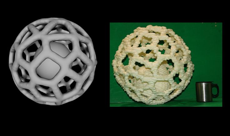 Creating biological materials with desired functions will lead to the fact that we can implant a freshly printed organ into a patient, rather than waiting for a potential donor to be decapitated in a car accident.
Made in the lab of Jennifer Lewis at Harvard University, this multicolored grid demonstrates the possibilities of multi-material printing.
Despite all the excitement and expectations from 3D printing, endless discussions and plans, the possibilities of technology are still extremely limited. This was very well written in this habrapost: the problem is in the dimension, I advise you to look and read in more detail. At the moment, printers can print complex shapes, but most often from plastic or from several types of metal alloys. But what if it becomes possible to use various materials, from living cells to semiconductors, so that the printer can mix such ink with the highest precision?
Jennifer Lewis of Harvard University is working on this problem.![]() It prints objects of complex shape, adding to them materials useful for the mechanical properties of the object, its electrical conductivity or optical characteristics. This will allow technology to move to a new level: the level of creating objects that can respond to the environment.
It prints objects of complex shape, adding to them materials useful for the mechanical properties of the object, its electrical conductivity or optical characteristics. This will allow technology to move to a new level: the level of creating objects that can respond to the environment.
Four types of resin inks of different colors were used for the demonstration. Multicolored ink placed in 9 standard printheads0010
Consistently and accurately, the machine created a colorful grid. Special software was used.
As you may remember, Princeton printed the bionic ear and Cambridge printed retinal cells for eye surgery. But the Lewis lab has outperformed everyone so far.
Last year, Lewis and his students printed microscopic electrodes and other components for a miniature lithium-ion battery. Another project was plastic-backed sensors capable of detecting an athlete's concussion.
More recently, they have printed biological tissue with a complex network of blood vessels woven into it. To do this, the inks were made from different types of cells and materials that form the matrix that supports them. What for? To more effectively test drugs on living tissue, or perhaps to create artificial organs for humans.
Silver nanoparticle ink is used to print electrodes smaller than a few micrometers. The process is controlled by special software.
On the left is Jennifer Lewis. On the right is a glove with a strain sensor, created by "imprinting" electronics into an elastomer.
Lewis' secret is that all ink can be used during the process. Although the inks are made of different materials, they can all be used at room temperature. It is also worth mentioning that when working with different materials, problems arise: for example, the cells are too thin and can be destroyed at the outlet of the nozzle. Therefore, you need to think about how else to "squeeze" them to the right place. Work continues.
3D printing offers help to the semiconductor industry
At this stage in its development, additive manufacturing (AM) and 3D printing extend far beyond the aerospace sector that pioneered them. Technology is penetrating the automotive, energy, education, medical and other industries. The list includes the semiconductor industry, where sophisticated equipment can take advantage of the benefits that AM brings to other areas. For example, improved efficiency, customized production and innovative design capabilities.
Benefits of 3D printing in industry
Today, there are five leading chip manufacturers:
• Intel,
• Samsung,
• NVIDIA,
• Texas Instruments,
• Broadcom.
They rely on a wide range of contractors, subcontractors and vendors to create each component that the board installs. And it all depends on those who produce raw materials. Due to the long supply chain, semiconductor manufacturers can easily be hit by major issues such as the COVID-19 pandemic.or a ship stuck in the Suez Canal.
Photo: 3DSystems
The electronics sector is innovating as quickly as possible to keep up with Moore's Law and growing industries that rely on a steady supply of new, better, and smaller chips. The pandemic is also encouraging businesses, educational institutions and people to go online more. Schools buy tablets, computers and upgrade local networks. People work remotely, but most SMBs are not connected to the cloud. At the same time, large server firms and large-scale companies (Amazon or Azure) provide cloud services with increased load capacity.
All of this is causing disruptions in the supply chain as goods run out, requiring new supplies to keep up with demand. The situation has been exacerbated by deteriorating working conditions, restrictions, global economic problems and pandemic-related transport disruptions.
Semiconductor manufacturers have found that they can benefit by adopting a technology that can consistently and quickly produce models on demand.
Plastic prototyping is widely used in most high-tech industries, including semiconductor manufacturing. Metal 3D printing of finished parts is gaining ground. There are already wafer processing systems that include components fabricated on 3D Systems equipment.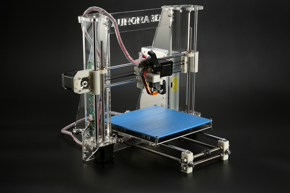 The company is increasing the share of 3D printing of parts on advanced equipment with each generation. There is now a doubling in the number of additively manufactured products within the brand.
Wafer manufacturers are trying to optimize systems to reduce interference and internal uncertainty in order to get to market faster. This requires a technology that facilitates the rapid improvement of prototypes. 3D Systems Direct Metal Printing (DMP) is a variation of the laser powder fusion process used by some customers to develop new designs.
Photo: Bart van Overbeeke Fotografie / ASML / Handout
Manufactured parts that reduce tool costs by combining multiple components into a single assembly. These include wafers with complex cooling channels that can be 5 to 7 pieces machined and soldered together and take two to three months to make. With the help of AP, this node can be made more efficiently as a whole and with improved performance. Various materials can be tested for the best thermal performance: copper, aluminum or titanium. This allows manufacturers to develop complex designs instead of first making manufacturing compromises and then sacrificing functionality due to these limitations.
Ways to optimize
Industrial application of 3D printing starts when a customer sees and addresses use cases for 3D Systems technologies, or a user encounters technical problems and sees an opportunity to overcome them with AM.
Photo: 3DSystems
3D Systems works with customers on obvious and achievable goals, including plates, manifolds and overall design optimization. The company has conducted research on the most sophisticated piece of equipment on the planet, the Large Hadron Collider. The apparatus is regarded as a leading example for the semiconductor industry with a base designed for particle mass physics experiments. The Dutch National Institute for Subatomic Physics sought to create sealed cooling rods that could reach -40°C in a particle accelerator detector. Fabrication of the component using conventional processes was not possible due to the necessary wall thickness needed to minimize the amount of material between the coolant and the surface to be cooled.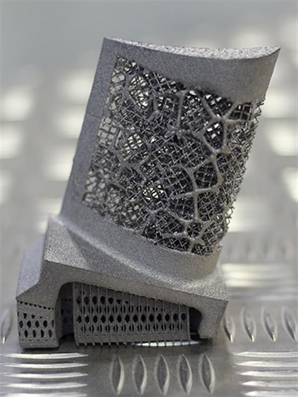 Working with 3D Systems, the scientists were able to fabricate rods from TiGr23. Sealed products had a wall thickness of only 0.25 mm with an accuracy of 50 microns with a part length of 263 mm. Over 300 cooling rods have been 3D printed using DMP 3D Systems technology.
Photo: 3DSystems
Another example. Wilting, a Tier 1 supplier to semiconductor manufacturers, has worked with 3D Systems to optimize fluid and gas flow in manifolds to reduce pressure drops as well as mechanical disturbance and vibration. The use of additive manufacturing to create pipelines has helped to reduce the perturbing forces caused by the liquid by 90%. In addition, converting a multi-part assembly into a single 3D printed manifold reduced the weight by 50%. This has resulted in improved reliability, performance and efficiency. The success of the partnership has led to increased demand for 3D printing in the industry with Wilting.
Modern equipment, low cost, high speed, reasonable power consumption are all key values, so the expansion of AM in the semiconductor field is inevitable.