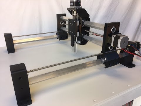
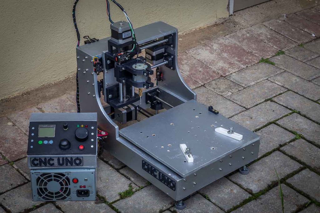
3D printer pcb milling
Free STL file CNC PCB milling machine
2-colour 3D printer
Free
GRBL + SD Card + LCD Screen + Keyboard
Free
CNC milling machine with LCD screen and SD card reader Firmware Marlin or GRBL
Free
Arduino 6-axis robotic arm
Free
Cardan coupling for 3D printer
Free
Cutting Plotter Flatbed Plotter 350x530 Marlin or GRBL
Free
Cutting Plotter or plotter width 310mm marlin or GRBL
Free
3D 3-wire 3-colour printer up to 16 colours
Free
Best 3D printer files of the Tools category
Bottle Bong
€2. 79
ski vices ;ski waxing support
Free
Temperature test - PLA version
Free
Marking Gauge with Folding Ruler (Customizable)
Free
Proton - Open Source 3D Printer
Free
Lola Animatronic Driod
Free
Spool holder
Free
Best sellers of the category Tools
Ender 3 Briss fang Gen2, Red lizard, spider, nf crazy, dragonfly, etc.
€1.87
Grinder | Grinder
€1.50
The Business Card Embosser System
€3
BMG E3D V6 Direct Drive for Creality Ender 3 (Pro/V2) & CR-10
€4.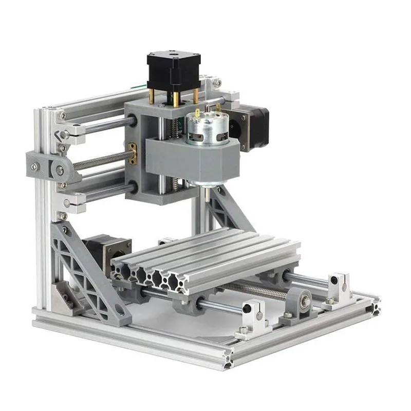 49
49
ENDER 3 S1/PRO SPRITE, 4020 FAN CR TOUCH NO Y OFFSET
€1.94 -15% €1.65
SUPERBOX
€1.50
well-engineered: Hemera fan duct
€2.50
Scissor Paint Rack
€5.66
GEARS & TRACTION MECHANISM
€3.59
Ratchet Holders - magnetic - toolbox organization stands
€2.91
NEW GENERATION HOLDER CAR PHONE HOLDER
€2.50
Chill Buddy Lighter Case
€1.02
UNIVERSAL INDICATOR FOR BED LEVELING FOR ALMOST ALL PRINTERS
€3.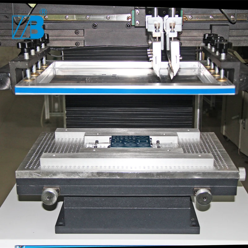 07
07
Minimus Hotend Cooler System
€2.57 -20% €2.06
Ender 3, 3 V2, 3 pro, 3 max, dual 40mm axial fan hot end duct / fang. CR-10, Micro Swiss direct drive and bowden compatible. No support needed for printing
€1.68
PET-Machine, make Your own filament from plastic bottles at home!
€50 -70% €15
Would you like to support Cults?
You like Cults and you want to help us continue the adventure independently? Please note that we are a small team of 3 people, therefore it is very simple to support us to maintain the activity and create future developments.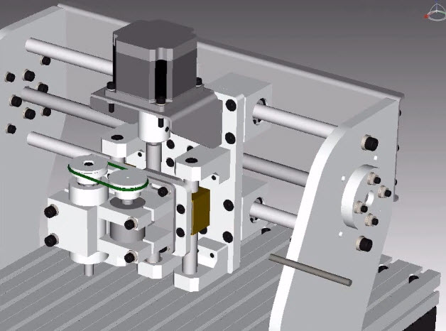 Here are 4 solutions accessible to all:
ADVERTISING: Disable your AdBlock banner blocker and click on our banner ads.
AFFILIATION: Make your purchases online by clicking on our affiliate links here Amazon.
DONATE: If you want, you can make a donation via PayPal.
WORD OF MOUTH: Invite your friends to come, discover the platform and the magnificent 3D files shared by the community!
3D printing, Printers Products Category on Adafruit Industries
Product ID: 1760
New from Printrbot, the Metal Simple is a brand new rock solid, all metal, fully-assembled Printrbot Simple! As opposed to the Printrbot Simple Kit, all of the laser cut wood parts have been replaced by rock solid metal and assembled. In fact, the total number of parts have been reduced to just a fraction of the wooden model. The all metal construction combined with.. .
.
More Info, PrintrBot Simple Metal 3D Printer - Black - Assembled
Product ID: 2323
The Othermill Pro is a portable, precise milling machine that allows you to create 2D and 3D objects out of durable materials, such as wood, metal, and plastic, using digital designs. It's one of Lady Ada's favorite tools, and we use one at the Adafruit factory every single day to prototype new designs, create testers, and experiment with fun new materials This...
More Info, Othermill Pro - Compact Precision CNC + PCB Milling Machine
Product ID: 1735
The Printrbot Simple is an exercise in 3D printing minimalism. It includes only what is needed to get started in the world of 3D printing. After building this kit you'll have a fully-functioning 3D printer that weighs only 10 lbs and fits nicely on your desk Please note! the Printrbot is a kit and not for beginners! You'll get all the parts to assemble your own 3D...
More Info, Printrbot Simple Kit - 1405 Model
Product ID: 2302
New from Printrbot, the Metal Plus is a rock solid, all metal, fully-assembled beast of a printer! The new Printrbot Metal Plus w/ Heated Bed is constructed of powder coated metal and machined aluminum with open platform for fabricating parts up to 10 x 10 x 10 inches using 1. 75mm PLA filament (As opposed to the 6 x 6 x 6 inch build volume of the cheaper Printrbot...
More Info, PrintrBot Metal PLUS 3D Printer - Black Assembled - Heated Bed - Model 1504
Product ID: 2412
Built to last and better than ever. The Series 1 Pro 3D printers from Type A Machines offer durability, modularity and one of the largest build volumes in their class. Featuring a streamlined aluminum and acrylic body, a glass build surface and a precision laser cut CNC folded metal chassis, the Series 1 Pro pushes the envelope in desktop 3D printing by matching a...
More Info, Type A Machines Series 1 Pro 3D Printer
Product ID: 2259
The ORION™ Delta 3D Printer is an exciting and attractive new 3D printer from the folks at SeeMe CNC that's designed to print ABS, PLA, and other materials from the very beginning. There's no need to refine or do anything to your printer - so you really have a ton more options for material than you usually do with an unmodified 3D printer. There's also an up-front...
More Info, ORION™ Delta 3D Printer - Black
Product ID: 2673
The Ultimaker 2+ is one of our favorite 3D printers on the market. It's a well-built open-source compact machine with an excellent UX. Every inch of the Ultimaker 2+ is designed to create the most effortless and reliable 3D printing experience ever! Click here for helpful tips! Ultimaker also created Cura, the open-source software that most other manufacturers use,...
More Info, Ultimaker 2+ 3D Printer
Product ID: 2742
The Flashforge Creator Pro is the latest addition to FlashForge’s Creator family, built upon an open source platform. Based on proven design of the Creator X chassis, the Pro is now enclosed so you can print ABS better and more efficient than ever. The upgraded three-point platform leveling system is now more intuitive than ever and the all-new heat resistant...
More Info, Flashforge Creator PRO
Product ID: 3528
This is quite the snazzy lookin' 3D printer – and it comes all the way from beautiful Barcelona.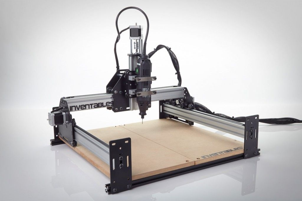 It's the BCN3D Sigma 3D Printer! It has a unique, Independent Dual Extruder system that allows you to print two (2!) different materials or colors while ensuring the finest surface finish. The idle toolhead remains parked, preventing the dripping of molten plastic...
More Info, BCN3D Sigma 3D Printer
Product ID: 3897
The Monoprice Inventor II 3D Printer Touchscreen with WiFi is a perfect entry-level 3D printer with small footprint and reliable performance. It comes equipped with WiFi so you don't need a cable tether and a lovely 3.5" color touchscreen for settings & feedback. The chassis housing is enclosed to keep your prints safe, and if you wanted to upgrade this printer...
More Info, Monoprice Inventor II 3D Printer with Touchscreen and WiFi
Product ID: 2933
The magic of 3D printing is now more affordable and accessible than ever! Meet The Micro 3D Printer by M3D, the first truly consumer 3D printer. Sporting a compact design, user-friendly software, and replaceable print beds and nozzles, it’s perfect for beginners and experts alike.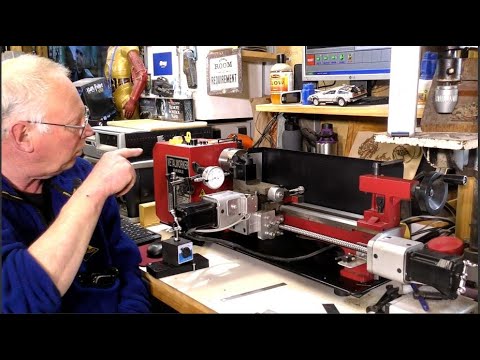 This is the Micro 3D Printer - Black - Retail Edition which is more like a...
More Info, Micro 3D Printer - Black - Retail Edition
Product ID: 3300
The Ultimaker 3 is one of our favorite 3D printers on the market. It's a well-built open-source compact machine with an excellent UX. Every inch of the Ultimaker 3 is designed to create the most effortless and reliable 3D printing experience ever! Click here for helpful tips! The dual extruder features swappable “print cores” which allows you to use...
More Info, Ultimaker 3 - 3D Printer
3D printing in radio electronics / Sudo Null IT News But often people go too far in their search for new applications for 3D printing. Let's touch on the topic of production of printed circuit boards and REA cases using 3D printers today.
To begin with, we will consider all methods for creating printed circuit boards (hereinafter referred to as PCB).
PP production
Radio electronics enthusiasts often dream of some kind of device for the production of printed circuit boards at home.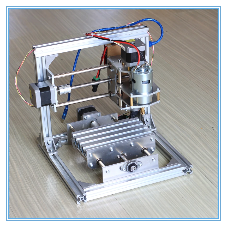 Of course, there is the great “LUT” technology (laser ironing technology), as well as the classic photoresist. But often too lazy to mess around with all this, I want someone to do everything for you.
And there are several ways to create PCB:
- Removing the conductive layer. Milling or scraping the copper layer of fiberglass
- Removing the protective layer from the surface of fiberglass
- Photoresist exposure
- Applying a protective layer on fiberglass
- Direct printing of conductive and dielectric tracks on the surface of various materials
- Filling cavities with conductive material
Remove conductive layer. Milling or scraping the copper layer of fiberglass
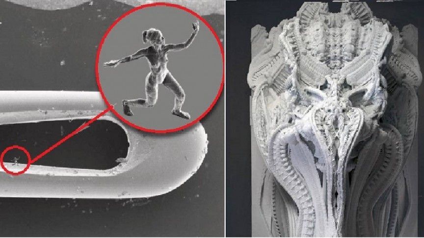
This method is the simplest, and even a very flimsy and cheap router can handle this task. Many enthusiasts even put a small engraver on their 3D printers and successfully mill PCB. (Looking ahead, let's say that a 3D printer-based router is only capable of milling PCB, nothing more.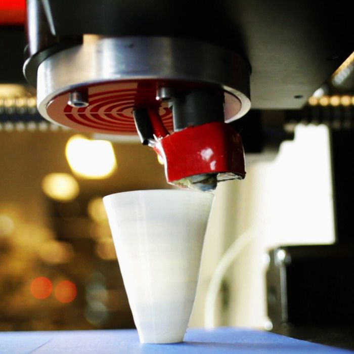 A router and a 3D printer are different devices, although many manufacturers try to combine them).
» Roland EGX-350
Working area: 305 x 230 x 40 mm; Spindle power: 50W, 20000 rpm; Number of axles: 3
The EGX-350 is Roland's most popular engraving machine. With its compact size, complete non-ferrous metal engraving capability, high-speed spindle up to 20,000 rpm, and curved surface engraving, the EGX-350 finds applications in a variety of applications from printing plates, promotional merchandise engraving, creating wax master models in jewelry, and also used in mechanical engineering for marking, engraving printed circuit boards and electrodes for electroerosion, and much more.
» Roland EGX-400
Working area: 407 x 305 x 42.5 mm; Spindle power: 72 W, 30000 rpm; Number of axles: 3
The EGX-400 is Roland's professional engraving machine, designed specifically for high-speed engraving.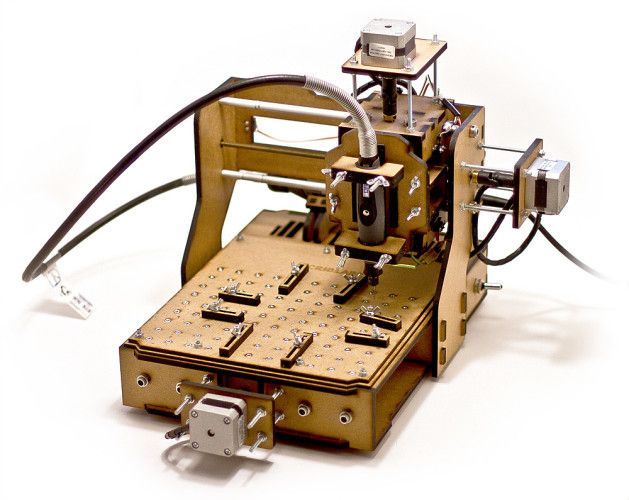 With a high-speed spindle up to 30,000 RPM, servo motors in all axes, and FFP (Feed Forward Processing) technology that scans the program several steps ahead and achieves high speed and smooth movement in curves, the Roland EGX-400 is a leader in its class
» Roland EGX-600
Working area: 610 x 407 x 42.5 mm; Spindle power: 70W, 30000 rpm; Number of axes: 3
The EGX-600 is Roland's CAMM-2 PRO series of powerful, high-precision servo engraving machines for professional 2D/3D engraving and milling at an affordable price. EGX PRO is a series of engraving machines equipped with advanced industrial technology with the power, table size and speed of professional engraving machines, but at affordable prices. The EGX-600 is equipped with a 70W spindle and 30,000 rpm. The EGX-600 is ideal for making high precision embossing and embossing dies. In addition, the machines engrave nameplates, tags, medallions, 3D inscriptions, dashboards, printed circuit boards and more.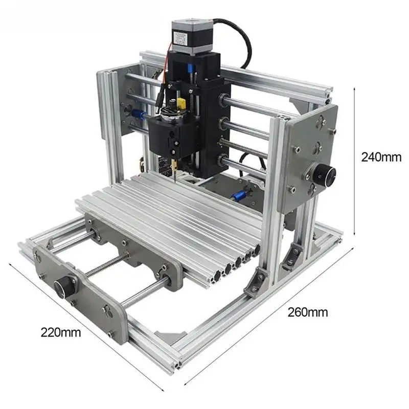
As you can see, the machines are not the cheapest, and few radio amateurs can afford them. But still, the instructions for preparing the circuit for milling in this article: “A printed circuit board at home, or how to make a printed circuit board at home using a CNC machine.”
This method is not limited to one router, you can also use a sufficiently powerful laser to burn the tracks, or scratch the tracks with a needle. And also use the method of electroerosion.
Laser engraved PP
The last method is rather controversial and more suitable for the next method.
Removing the protective layer from the surface of fiberglass
Just the method of removing paint with a needle is demonstrated in this video:
A permanent marker is used as a protective layer, and the machine itself is nothing more than a 3D printer.
In the same way, any laser module can be used to burn through the upper protective layer, followed by etching.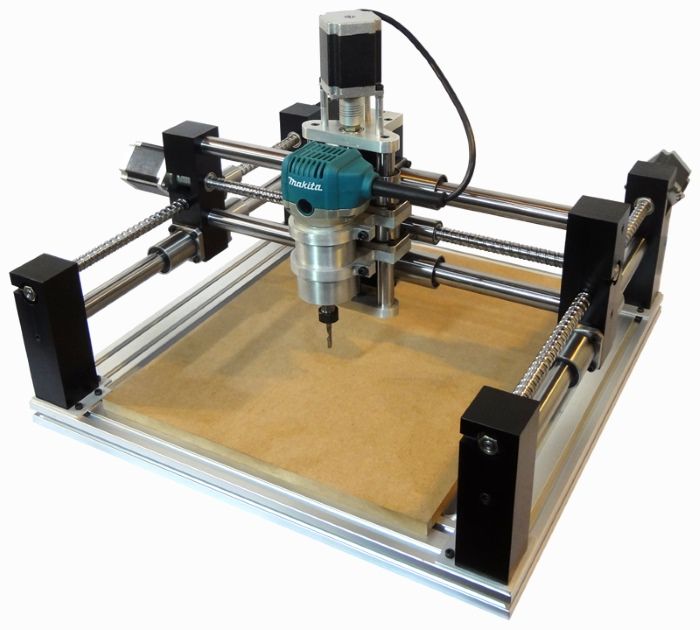
Photoresist exposure
It would seem that this method has long been known and what can be invented new? But here, any CNC device comes to our aid. After all, a laser can not only burn a board or a protective layer, but also illuminate the necessary sections of our board with a photoresist. Here are a few projects for example:
LaserExposer - a laser scan from the printer is used to obtain an image. with just a little magic, you can make a good photopolymer 3D printer out of this device.
DiyouPCB - in this case, mechanics and electronics are simpler. But the same principle is used. The laser diode is taken from the BlueRay drive head.
Applying a protective layer on fiberglass
This method can be called one of the simplest, instead of an engraver, laser or print head, we attach a regular permanent marker and draw our board. Despite the simplicity in this way it is very difficult to breed a board with thin tracks, the only limitation is the thickness of the marker rod.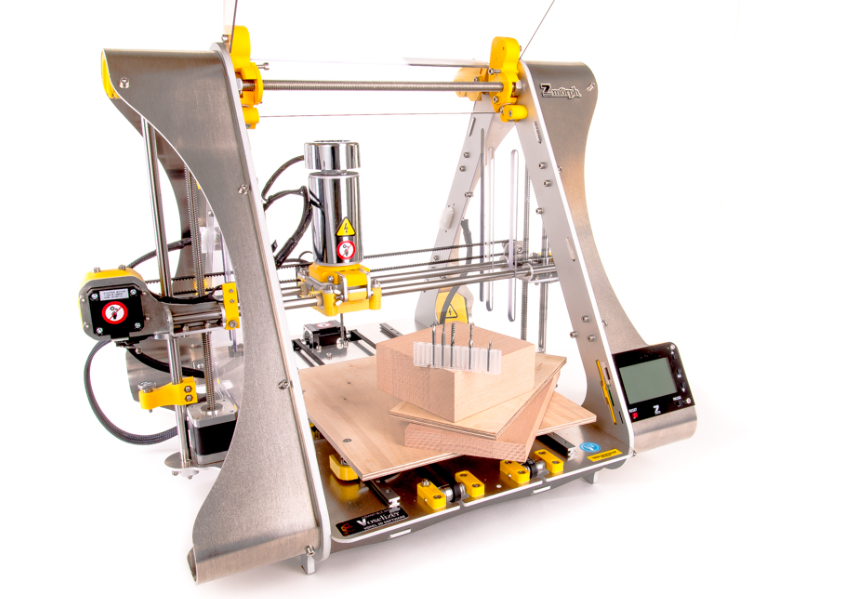
Don't forget about our old friend, the regular inkjet paper printer, many convert old technique to print on T-shirts or printed circuit boards. Read more in the article ”Direct Inkjet Printing of PCB Pattern”.
Direct printing of conductive and dielectric tracks on the surface of various materials
The method closest to the topic of 3D printing for creating PCBs and, in some cases, cases right away. Let's start with the simplest devices:
Drawing on the textolite surface allows not only applying a protective layer, but also “printing out” a conductive one.
https://www.youtube.com/watch?v=w_SC7YzHa-8
As you know, graphite is a conductor, which allows you to draw a printed circuit board on a sheet of paper. Yes, graphite is not the best conductor and almost certainly such a board will not work, but a pencil can be replaced with a marker with silver ink, as was implemented in the Ex1 PCB
printer
And coming very close to 3D printers, we want to present you two similar projects:
Voltera: Your Circuit Board Prototyping Machine is a device that can print with conductive paste or apply solder for baking in an oven.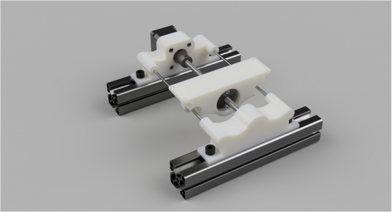
Voxel8 - this device uses the same principle of applying conductors, but immediately prints the body around them. It looks like an integrated circuit. The company demonstrated the potential of this technology using the example of printing a small quadcopter. Undoubtedly, this approach can open up new horizons for creating complex multidimensional circuits and entire devices, but so far this technique has a number of limitations. For example, a fairly large installation and thick, voluminous tracks, you can not use a soldering iron.
By the way, do not discount conductive plastics, and on a two-nozzle printer it is quite possible to print plastic circuits that are quite suitable for training.
Filling cavities with conductive material
And the last method, a little clumsy, but it has a place to be. It does not allow to obtain thin and compact boards, or multilayer ones. And also completely eliminates the effects of high temperatures, they can not be soldered.
As you can see, a cheap home printer can be quite successfully used to make PCB, converting it into an engraver (laser or milling), or directly print boards with plastic or paste. It is worth paying your attention to the fact that all of the above methods do not allow the full production of multilayer PCBs, which is a stumbling block for many radio amateurs. We hope that this problem will be successfully solved soon.
Well, the use of 3D printers does not end there.
REA housings
If everything is more or less clear with PP, and even without sophisticated devices for automatically creating boards, you can always return to LUT. That with cases for devices often there are problems. Of course, there are standard REA cases, but they are far from always suitable for homemade products, they require strict adherence to the size of the board and elements, which is not always convenient. Also, do not forget about the aesthetic side of the issue. In this case, a regular FDM 3D printer helps us perfectly. The only question is whether any printer is suitable for these tasks.
During the preparation of this article, tiger kindly shared his experience. further from his words:
“Once I had the experience of thoroughly getting to know this issue. The company was given the task of developing a CEA case in the form of a ladybug with further manufacturing of a mold for injection molding machines. As you understand, the task is still the same, this case had to look like a cow, while it was necessary to fit a standard square board inside the case. The modeling process did not take long, but an unexpected problem arose during the creation of a prototype. At that moment, our stratasys dimension broke down and we had to order printing on the side. We printed this body of PLA plastic with insoluble supports, and a thick layer. I had to apply putty and finish the model manually for a long time.
Then, of course, we printed the rest of the models on a refurbished stratasys, and completely finished with the case design. Later, the 3D model went to the factory. where the mold has already been made.
From this story it can be seen that not all cases are printed without problems, and often printing with soluble supports is simply necessary. Picaso Designer PRO 250 is ideal for such products.
For example, this case is printed on Picaso Designer Pro250 with two ABS+HIPS materials.
Agree, high-quality printing of such complex engineering parts without soluble support is almost impossible.
Large batch of business card holders, which can also be successfully used as a “third hand” for wires. As you can see, 3D printers are not limited to CEA housings.
For vaping enthusiasts, a 3d printer can also be useful when designing homemade box mods.
Also, do not forget about such body elements as latches, thin partitions, etc. These elements, even perfect FDM printers, do not print perfectly, and they cannot withstand the loads that molded parts can withstand. In this case, SLA printers save the situation, for example, the well-known Form 2. And using burn-out photopolymers, you can cast the body of your product from metal (even precious).
In this picture, on the right, the original part from ligitech headphones, as we can see, just thin latches are broken. This do was scanned and printed on a Formlabs Form2 3D printer.
Do not forget that the products printed on the Formlabs Form2 photopolymer printer require almost no post-processing, you immediately get a product of unsurpassed quality. This printer allows you to create a master model for casting cases without additional processing, as an example, the case we printed in maximum detail:
With subsequent casting into silicone:
And a few more cases. Without knowing in advance, few people will distinguish these products from the factory ones.
It is also worth noting that there are different polymers that differ in physical, chemical and optical properties.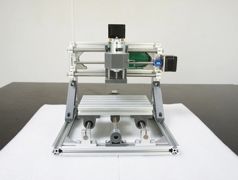 So we can immediately print some parts of the devices transparent.
Want more exciting news from the world of 3D technology?
Follow us on social media networks:
Printed circuit boards using a photopolymer 3D printer / Sudo Null IT News And in the last year or two, thanks to a strong reduction in cost, their photopolymer subspecies is also flourishing. Now such a printer is already available to almost everyone, and the number of their models on the market is multiplying every month.
Even when a few years ago I only learned about the emergence of a new type of photopolymer printers - in which the image of the layer for illumination is formed by the LCD, the thought flashed through me already then: "Hmm, what if we substitute a photoresist on a textolite?". But then it was a purely theoretical question - the prices for them were considerable, and the resolution and display area left much to be desired. However, today these printers can already boast of a decent resolution - from 30 microns per pixel, and a completely normal display area.
And as it turned out, with the help of an inexpensive modern photopolymer printer, it is quite possible to make boards with tracks / gaps from 0.15 mm.
I apologize in advance for such a voluminous graphomaniac, I myself did not expect that the note would get so fat...
I foresee the question "But why? In China, they will make normal boards with a mask and silk-screen printing for a penny!" I answer: now, most likely, there will be several iterations of finishing the board to a satisfactory state. I made a board - tested it - made corrections. And so several times. Waiting every time for 2-3 weeks from China is not an option :) But when the final design of the board is determined - then, of course, normal production in China or on Rezonit.
And now to business.
Who does not know - here is a brief principle of operation of such a printer The main part of such a printer is an LCD display. Below this display is a 405 nm UV source. Above the display is a bath of photopolymer, which has a thin transparent FEP film as a bottom. A platform is lowered into the bath, on which the model is “grown”. At the beginning of printing, the platform lowers to the height of one layer from the film, the image of the first layer is displayed on the display, and UV illumination is turned on for a specified time. Illumination, getting through the "open" pixels of the display and the film onto the photopolymer, hardens it, so a hardened layer is obtained. The first layer sticks to the platform. Then the illumination is turned off, the platform rises to the height of the next layer, the image of this layer is displayed on the display, and the illumination is turned on. The second layer is cured by welding with the previous layer. And this is repeated over and over until the entire model is printed.
The idea to try to make a printed circuit board using such a printer came to me again about three years ago, when I bought myself an Anycubic Photon S printer. , then I just forgot about this idea, because and there was no need to make boards. But the other day, the need arose for the manufacture of several small boards, and with a high probability that as tests are made, changes will be made to these boards and it will be necessary to go through several iterations of "manufactured-checked-changed" in a short time. And the idea resurfaced.
To be honest, I thought that by now the Internet would be filled with the results of such experiments, the idea lies on the surface :) But to my surprise I found that the Internet is almost completely silent on this issue. There are separate notes, but there is no integrity and completeness in them. That's why I decided to publish this post - maybe it will help someone go all the way faster than me, and with fewer rakes :)
Well, the most important thing is that you don't need film and you don't have to struggle with increasing the contrast of the template. You also do not need a separate UV source with a place for its installation. And, of course, it is stylish, fashionable, youthful.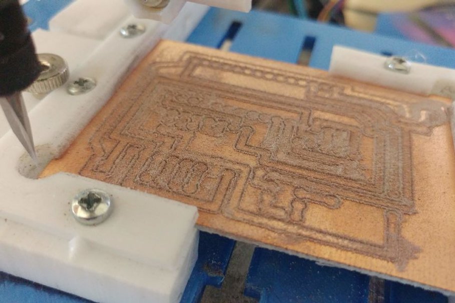
There are also disadvantages - the resolution of most modern 3D printers still does not cause much enthusiasm yet - the pixel size of all fluctuates around 0.05 mm. But this is already enough for confident manufacturing of boards with tracks from 0.2 mm and rather high chances of success with tracks from 0.15 mm. Due to the raster nature of such a template output, the position and size of elements on it can vary + -1 pixel, so I think it’s not even worth counting on tracks of 0.1 mm or less.
Let's go in order.
Task
It is necessary to make a printed circuit board at home using photoresist. Instead of templates and illumination lamps, use a photopolymer 3D printer that will serve both at the same time.
Let's divide the problem into separate steps-solutions for each moment.
-
Board development
-
Printer-friendly output of layers
-
Preparation of textolite with photoresist
-
Printer flare
-
Photoresist development, board etching
1.
 PCB development
 Well, there are no questions. Whoever prefers to work in what program - in that one makes boards. The main thing is that the program should be able to display the result in some commonly used form. The easiest way I've come up with is outputting board layers to gerber files that can be fed to an online service. But you can also output to PDF or images.
2. Converting the CAD output to a printer-readable form
This is where things get tricky. If almost all CADs can output to generally accepted formats - gerberas, DXF, printing to PDF, then 3D printer manufacturers so far categorically refuse to accept any file standard. Everyone is perverted as they can. The situation is largely saved by the fact that many manufacturers use motherboards from one Chinese company, Chitu Systems, in their printers. Thanks to this, many printers on such boards are able to understand one of the basic formats developed by the same company. And even often, if a file has some unique extension, then in fact it has the same basic format, just with a different extension.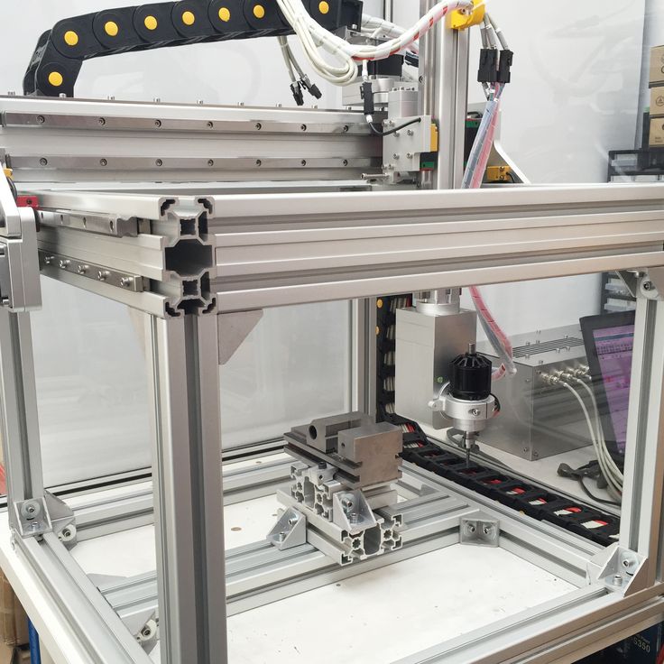 But it may differ in some details.
In any case, there is a free UVtools utility known among photopolymerists that can open files in one format and convert them to another format. It understands almost all formats on the market :)
I have tried two ways of preparing files with layers for the printer and I will describe both.
2.1 Gerber output and conversion to .photon
The .photon file format is understood by the old Anycubic printers - Photon and Photon S. This is exactly the case when the printer manufacturer took the format from Chitu and changed its extension. In the original, this is the Chituvian .cbddlp format, so you can safely change the extensions of these types of files among themselves and the printers will devour them like native ones.
Since I have a printer that understands this format, this method suited me perfectly. The limitations of this method are that the printer must understand .photon or .cbddlp files and have a display standard for most non-monochrome printers with a resolution of 2560x1440 and a diagonal of 5.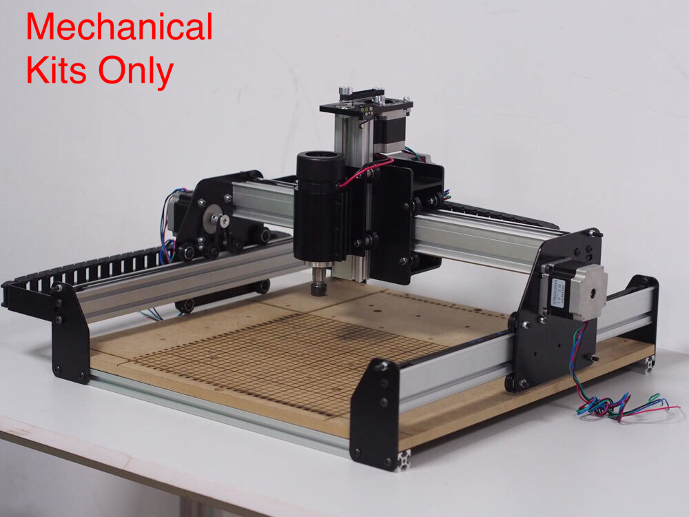 5". manuals on how to do this for any CAD that can, in principle, mirror layers or not - it makes no difference, they can be mirrored in the utility during the conversion process.0005
Now open the online utility for converting gerber files - https://pcbprint.online/ and load the gerberas into it. By the way, this is a utility from a Russian developer who lives here.
It is easy to understand, although it does not contain any information or help. But I will give a short guide:
For a single-sided boardUpload your gerbera in the main window with the "Upload file" button:
We made sure that everything is fine and the image meets expectations, if necessary, make a negative or mirror the image with the buttons in the top center, and press the button " Render layout":
Now press "Lauout" at the top right and get into another screen:
Here you first need to go to the settings (gear button at the top right) and there select the format of the output file "photon":
The time in "Exposition" can be left at default and change it to the desired one directly in the printer. But you can immediately put the right one if its value is already known :)
Close the settings and return to the previous screen. Here the output image is on a black space showing the working field of the printer. The image can be moved, aligned. When everything suits, we first press "Render", and when the "Download result" button next to it becomes active, we also press it. And save the proposed .photon file to a convenient location on your computer :)
For double-sided boards, things are a little more complicated due to the need to match them. Therefore, it is necessary to know very exactly the position of the image displayed on the printer's display in order to place the board on the display very accurately in accordance with it.
I had several options for solving this issue, but in the end I decided on the simplest of them, which did not require any mechanical conductors. To do this, I still in CAD in a separate layer (it is possible in the border layer or in any other "unnecessary" layer) I draw a frame around the board with a line of 0. 15 mm and indented from the edges of the board by 0.25 mm. As a result, I get three gerberas - the top layer, the bottom layer and a separate empty frame.
I upload all three gerberas to the above site and then in a few steps I get three files for the printer.
Double-sided board in pcbprint.online/So, all three gerberas have been loaded. All of them are mixed together, but it's not scary:
Now hide the top and bottom layers, leaving only the frame (by clicking on the eyes in the names of the gerberas).
Click "Render layout" and go to the "Layout" screen with the button in the upper right corner. We see an empty frame, drag it to the desired position on the black field of the display, click "Render" and "Download". The first file for the printer is ready.
Switch back to the gerber screen with the "PCB comose" button. Redisplay the first layer (the frame layer still remains visible), mirror if necessary, and click "Render layout" again. Again we go to the output screen and now there are two pictures hanging on the display field - a separate frame and the first layer with a frame.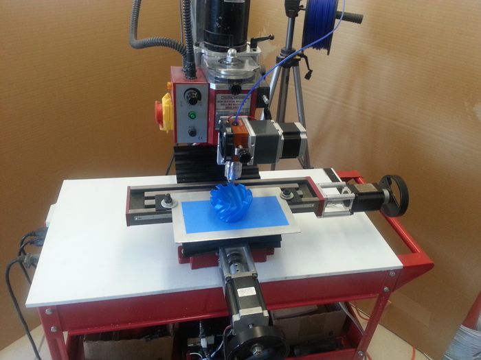 The frame remained in the same place where we pulled it last time. And now our task is to exactly combine the frame of the first layer and the empty frame:
Press "Increase" and combine in one of the corners. In this case, in no case should you move the empty frame that we set in the last step!
Combined, click "Render" and "Download", and we have a second file for the printer. Before returning to the gerbera screen, we delete the render layer with the frame, we should again have an empty frame. And now we return to the gerberas, hide the first layer and display the second one, look at the need to mirror, click "Render layout" and go to this screen again. In the same way, we combine the layer frame with an empty frame (which cannot be moved!), then "Render" and "Download".
Everything, all three necessary files for the printer are ready.
All this hemorrhoids allows you to generate for the printer files of an empty frame and layers with a frame in the same place on the printer display with high accuracy. The empty frame serves to aim the board, more on that below.
If necessary, the resulting .photon files can be converted to the desired format using UVtools :)
2.2 Output layers to PDF or images
The second method is perhaps more confusing, but its great advantage is versatility, it is suitable for any printers, whose formats are supported by UVtools. I will describe it only in general terms, because. There are quite a lot of tools and specific ways to implement it, and everyone can choose them according to their preferences.
So, the goal of the first step is to get a picture with a size equal to the resolution of the printer's display, preferably in a lossless compression format. In this case, the image of the layer in the picture must correspond to the real size in the scale of the display.
If CAD allows you to output directly to the picture - great, output to it. If the resolution of the output image is configurable - specify the resolution of the printer display. It is elementary to calculate it - we divide the number of pixels across the width of the display by the width of the working area in mm and multiply the result by 25.4, we get the resolution in pixels per inch. If the resolution is not set, then set the image size as large as possible so that there are at least 15-20 pixels per 1 mm of the board.
If output to image in CAD is not available, then output to PDF. This PDF will need to be opened in another program and converted to an image. Photoshop, Corel, maybe other programs can do this... The requirements for image resolution are the same. For example, in Photoshop, when importing a PDF, you can immediately specify with what resolution to convert to an image. For example, for common displays with a resolution of 2560x1440 and a diagonal of 5.5 "the resolution is approximately 537.566 PPI (pixel size - 0.04725 mm).
The resulting image will need to be changed in some image editor, bringing its size to the resolution of the printer's display. In this case, the layer image must be scaled to the real one (taking into account the pixel size of the printer display) or saved without scaling if the PPI of the display was specified when importing the image.
UPD: in the comments @0x3f00 gave a link to his converter of PNG images to files for the .photon printer - https://github.com/0x3f00/PhotonCpp/releases/tag/v1.0.0 . There is also an instruction for using it just for the purpose of manufacturing boards - https://github.com/borelg/PhotonPCB.
2.3 There is another way, but it is very resource-intensive
You can output layers to PDF, then open this PDF in Corel, convert it, save it in DXF, extract a three-dimensional object from this DXF, which you can push into the printer's slicer.
Necessary transformations in the vector editor:
-
Connect all curves.
-
Convert outlines to objects.
-
Merge intersecting objects.
You can extract a three-dimensional object from DXF, for example, SolidWorks. Fusion360 also seems to be able to. Who else is capable of this - I honestly don't know, but in theory any CAD that can import DXF as a sketch.
Thus, for example, I made a model for determining the exposure time of the photoresist.
3. Preparation of textolite with photoresist
The Internet is simply littered with articles on this topic, but for the sake of integrity and for the sake of some specific points, I will also describe such well-known stages as the preparation and etching of textolite.
My first experience with such a fabrication was a couple of days ago with a domestic photoresist PF-VShch. Taking into account the last yesterday's experience, I categorically advise not to waste time on this photoresist, but immediately take a decent one - Ordyl Alpha 350(330) :) They say that Kolon is also decent, but I have not tried it. With Ordyl photoresist, the results are much more stable and accurate, it is easier to develop and adheres much better to the foil. And he can forgive those mistakes that will be critical for the PF-VSC. And what is important - it is sold in a bunch of places quite inexpensively.
3.1 Preparing the textolite
To begin with, the textolite should be smooth, very preferably with a smooth foil without scratches or dents. Otherwise, the chances of success are reduced.
If a double-sided board is being made, then you need to immediately cut the board out of the PCB exactly to size. If there is any CNC router, then you can drill all the holes and cut along the contour in one installation, as I do. If not, then it is better to leave the drilling for later, when the board is etched.
After this, the textolite blank must be very carefully cleaned and degreased. This can be done with a kitchen abrasive sponge (but not used for washing dishes on which fats have already accumulated) and a scouring powder like Pemolux. Very carefully, slowly three every square millimeter of foil, without touching it with your fingers.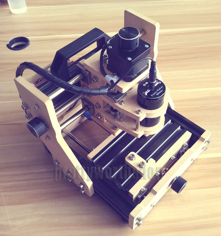 In general, I categorically do not advise touching the foil after the start of cleaning with your fingers, there should not be the slightest even the weakest greasy spot on it. After cleaning, rinse thoroughly under running water, shake off excess water and allow to dry. I do not advise blotting or wiping with anything, because. grease can be applied, even from a new napkin.
3.2 Application of photoresist
This is also a fairly common topic on the Internet, so I'll go over it briefly.
Photoresist usually comes in sheets or rolls. It consists of three layers - two protective films and the photoresist itself between them. A piece is cut off from the photoresist according to the size of the board + 5 mm in length and width, then a matte (polyethylene) protective film is removed from it.
the second, glossy (lavsan) must remain on it until the etching stage.
The easiest way to remove the film is with a piece of tape. It is glued with its edge to the corner of the photoresist and then folded back, pulling the protective film along with it.
After removing the matt film, the photoresist is applied to the edge of the board and smoothed along this edge with a finger. The rest of the photoresist is supported by weight, without tension, but in such a way that as little as possible of its area lies on the foil.
Please note that if Ordyl photoresist falls on a well-prepared textolite, it can stick to it tightly, and you won’t roll it without bubbles. You have to scrape it off and do it all over again. And PF-VShch can fall as much as you like - it definitely won't stick :)
Now the knurling itself. If you have a laminator, into which textolite will crawl through the thickness, then it's just wonderful. We make an envelope-type strip of paper folded in half, put a textolite with a sticky edge of the photoresist in it, and serve this sandwich into a laminator heated to 100-110 degrees. At the same time, we continue to hold the photoresist so that it comes into contact with the textolite foil only directly at the laminator inlet.
That's all for Ordyl, for PF-VShch it will be harmless to roll a couple more times.
If there is no laminator, then smooth the photoresist to the textolite with your finger from edge to edge, gradually lowering it onto the textolite. The main thing is not to catch the bubbles. After all the photoresist lay on the foil, we take a hair dryer and heat the textolite to 70 degrees, after which we iron the entire photoresist once again.
After knurling, let the textolite with photoresist lie down for 15-20 minutes, or at least until they cool down to room temperature - according to the recommendation of the photoresist manufacturer.
And now everything is ready to highlight the layer pattern :)
4. Printer highlights
I want to warn you right away: looking directly into the glowing display of a photopolymer printer may not be very good for the eyes. Although not true UV (405 nm), the brightness is quite noticeable and can be harmful to the eyes. Therefore, I recommend using colored or tinted goggles. I think even sunscreen will do.
To begin with, you need to remove the bath and platform from the printer, they are completely unnecessary for this business and even interfere. This completes the preparation of the printer :)
Lighting also has different options. If you have a one-sided board and the blank is larger than the size required for the board, then everything is simple - throw the file obtained at the preparation stage into the printer and, knowing the approximate place for displaying the image on the display, put a textolite with photoresist in this place. Then start printing the file and wait until it is completed. Everything, the photoresist is exposed, it is possible to develop.
If the workpiece is equal in size to the board being made and the error with the position of the workpiece on the display is unacceptable, then in this case it is necessary to remove the frame during preparation, as is the case for a double-sided board. Illumination also occurs using a frame, similar to a double-sided board, only without the second side and the second layer.
So, the illumination of the double-sided board. We throw all three files into the printer - with a frame, with the first layer and with the second layer. We put the workpiece next to the printer in quick accessibility. If it is already pre-drilled, it will be useful to make sure that it lies in the correct position so that you can quickly take it and immediately put it on the display. To do this, we run a file with a layer planned for exposure, and compare the layer pattern on the display and the orientation of the board next to the printer.
Printing a file with one frame. As soon as the frame lights up on the printer display, we take the workpiece and put it approximately inside the frame. While the frame is being illuminated, we align the workpiece so that it is exactly in the frame, with the same indentation of the frame from the edges of the workpiece on all sides.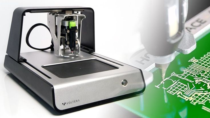
In the photo, I gave an example with a ready-made board, because I did not take pictures during the manufacturing process. Well, reflections interfere quite strongly, alas... But I think it's understandable :)
That's it, the position of the workpiece is verified, printing of the frame file can be interrupted or wait for it to finish. Without moving the workpiece, run the file with the first layer and wait for it to finish. We illuminate the second layer (the second side) in the same way - we launch the frame, place and align the workpiece, without moving it, we launch the second layer. Before this, just in case, you can make sure that the workpiece will lie in the correct orientation, as before the first layer.
If the workpiece is not completely flat and does not fit the entire area to the display, then you can press it down from above with some heavy flat piece of iron. You just need to make sure that this piece of iron does not interfere with the platform lever, which will go down with the start of printing - the printer thinks that this is a normal photopolymer print and you need to lower the platform to the bottom of the bath :)
Illumination time can be different from printer to printer .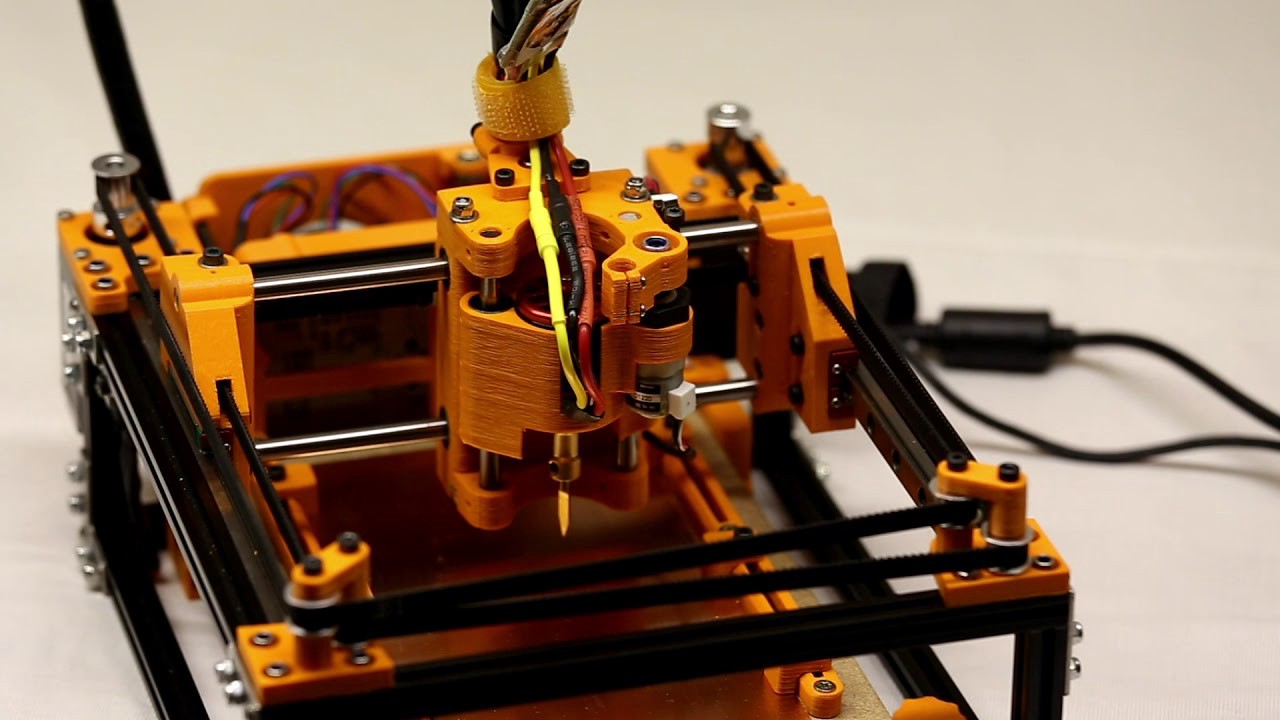 It depends on the power of the emitter, and on the optical illumination system, and on what type of display is worth - monochrome or RGB. Here already it is necessary to select each individually. For orientation, I can say that I got the best result with the Ordyl photoresist at an exposure time of about 90-110 seconds. With photoresist PF-VShch - about 10-13 minutes. Printer with paraled, illumination power slightly less than 50 watts.
After exposure, the workpiece should be allowed to rest for 15 minutes - this is according to the recommendation of the photoresist manufacturer. Ordyl changes the color of the highlights quite noticeably, so it's pretty easy to control the highlights. Unfortunately, the photo did not convey it well, it can be seen better with the eyes.
5. Development, etching
Everything here is according to the recommendation of the photoresist manufacturer and according to the classics of the Internet.
All necessary chemicals were purchased inexpensively from Auchan.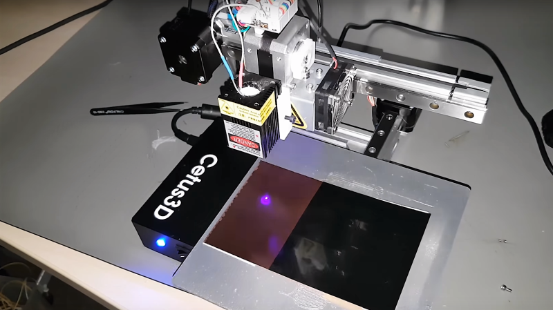 Even hydrogen peroxide 6% - this was a surprise for me, I had never seen it in hypermarkets before, and even in liter bottles.
For one session you need:
-
Soda ash - 1.5 grams
-
Hydrogen peroxide - 150 ml for 3% (or 75 ml for 6% + 75 ml of water)
5 grams -
Salt - 7.5 grams
-
Alkali (caustic soda, sodium hydroxide) 5-7% - 100 ml
With the cheapness and ease of buying all the components around the corner, I am in favor of preparing a new solution for each board. Although the etching solution, as they say, is not stored anyway. A solution of soda ash noticeably "poorer" in the process of development. Unless caustic soda can be reused, but is it worth it to keep another bottle ...
Both Ordyl and PF-VSH appear in a weak solution of soda ash. For PF-VShch - 1-2%, for Ordyl - 0.8-1.2%. For Ordyl, we take 150 ml of water and dilute 1.5 grams of soda in it. The solution can be heated up to 30 degrees, this will speed up the development, but it is important not to overdo it, otherwise the illuminated areas may begin to be damaged.
Ordyl appears rather quickly. Already after 10-15 seconds, the illuminated pattern begins to become more and more contrasty, the unexposed areas gradually dissolve, become thinner and become paler.
To speed up the process, it is recommended to shake the bath so that the reaction products are washed off the surface of the workpiece. For this I adapted my old 3D printer, its table and shook and heated the bath with the solution during development and etching :) Two minutes passed before there were at least some signs that development had begun. In addition, if Ordyl does dissolve, then PF-VShch first swelled like gelatin and discolored, and only then began to slowly dissolve.
At the end of development, you can go over the boards with a hard paintbrush (or soft toothbrush) several times in different directions to help wash out the remaining photoresist from narrow places. Ordyl holds on tight, this procedure should not disrupt it, but with PF-VShch you need to be very gentle, even without a brush it strives to exfoliate on thin paths.
After etching, the workpiece must be rinsed in cold water so that the soda residues do not continue to attack the photoresist and so as not to clog the etching solution with them.
The result should be something like this, maybe even better :)
More detailsScale of the grid square - 0.2 mm:
The scale is the same. Here you can see the raster component of the illumination, the pixels stick out:
Etching was also done according to the traditional recipe popular on the net:
It is better to heat the solution to 40-50 degrees, then the etching goes much faster. This is my first experience with this solution. I used to poison with ammonium perchlorate, and even earlier - with classic ferric chloride. To be honest, I can't really express how I feel about this solution. On the one hand, it poisons rather quickly, is transparent, does not get dirty, and is relatively safe. On the other hand, it seemed to me that it was easing quite a lot ... But maybe it just seemed, I haven’t been making boards for 10 years and I forgot how it all worked when the trees were big :)
After etching, the exposed photoresist must be removed from the workpiece, and this is done in caustic soda.
 On my bottle of cleaner it says "at least 5% but not more than 15%" and it takes 5-8% to remove the photoresist. I diluted the product 1:1 with water and this solution did the job perfectly. The photoresist does not dissolve in it, it simply peels off the foil after 2-3 minutes and begins to float in tatters in the solution.
 After that, the board is thoroughly rinsed under the tap and... The board is ready!
Summary of my experience
Overall I am satisfied. I did not expect to get tracks / gaps of 0.1 mm and I did not get them. Here, the capabilities of the printer are severely limited (pixel size), and in general, good experience is needed for such results. But I was hoping to get at least 0.2 mm, and if I'm lucky, then 0.15 mm - and I got it. 0.2 mm confidently, 0.15 mm - well, so-so... If you try, you can achieve :)
There were some flaws - it was not pickled in some areas, and imperfect alignment of layers and holes. But neither is critical. As for the non-mordant - I think that I just hurried to take it out of the developer, I was afraid after PF-VShch that thin paths would begin to peel off.
Learn more