3D printed integrated circuits
What's Possible Now and in the Future?
Ziv Cohen
Application Manager, Nano Dimension
The semiconductor industry gets a lot of attention—and for good reason. Integrated circuits make technology possible, and these devices are built on the back of semiconductors.
Semiconductor manufacturing processes have come a long way since Robert Noyce invented the integrated circuit in 1959. With the rise of Industry 4.0 and the wide array of additive manufacturing processes, one naturally wonders whether the electronics industry will advance to 3D printing integrated circuits at full scale.
In this discussion, the question naturally arises: Why use additive manufacturing processes to produce integrated circuits? 3D printing is already being used to produce fully-functional PCBs with unique geometry, interconnect architecture, and various levels of component embedding. The ability to 3D print integrated circuits and other semiconductor devices directly into a PCB allows low-volume fabrication of highly specialized devices with unique form factor and capabilities.
IC dies on a silicon wafer
The Current State of 3D Printing Integrated Circuits
Silicon, III-V, and II-VI semiconductor manufacturing processes are highly advanced and are used to produce integrated circuits with less than 10 nm gate sizes. Currently, the most advanced 3D printing processes provide near micron-level resolution and co-deposition of multiple materials.
Co-deposition is critical for 3D printing integrated circuits because conductors and semiconducting materials must be printed simultaneously. The resolution of the most advanced 3D printing systems must still improve before VLSI is possible. In addition to improving device performance, miniaturization will provide much lower power consumption for switching logic gates.
As an example of what is currently possible with 3D printing integrated circuits, researchers at the Air Force Research Laboratory and American Semiconductor recently 3D printed microcontroller SoCs from polymers on a flexible silicon substrate.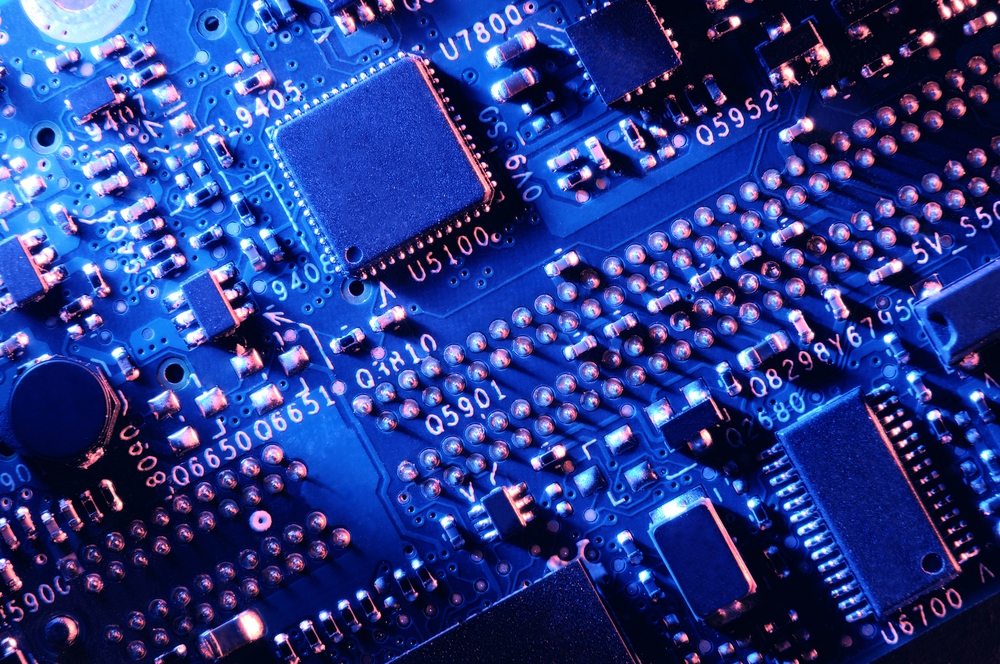 These microcontroller units offer 7000x memory compared to other flexible integrated circuits at the time. Some envisioned applications include environmental or strain sensing, as well as munitions inventory monitoring.
A flexible microcontroller integrated circuit. This circuit was fabricated using polymers on silicon.
Currently, thin-film transistors (TFTs), diodes, LEDs, can be 3D printed from organic polymers with commercially available and experimental systems. The 3D-printed TFTs can have various contact/gate configurations and can easily be scaled horizontally and vertically. Polymers can be easily doped and functionalized, allowing their electronic and optical properties to be tuned to meet the demands of different devices.
Using polymers on a semiconductor wafer is a natural route to pursue 3D printing integrated circuits. Electrical contacts can already be deposited in an additive manner through a mask (i.e., thermal evaporation, PVD, or CVD), followed by deposition of semiconducting polymers and larger conductive tracks with a 3D printer. Their adaptability to low-temperature processes also makes them ideal for 3D printing integrated circuits directly on standard semiconductor wafers.
Other researchers are working on advancing additive manufacturing processes and materials to enable 3D printing integrated circuits. As an example, the University of Hamburg and Deutsches Elektronen-Synchrotron developed a 3D printing process that can enable the fabrication of integrated circuits. This process uses a mesh of ~20 nm silver nanowires as conductive elements and a thin film of polymer as an insulator or semiconducting material. This process is still in the research phase, but it illustrates how unique nanostructures can be used to fabricate semiconductor devices that rival silicon integrated circuits.
The Economics of 3D Printing Integrated Circuits
In any manufacturing process, the cost structure involved in manufacturing is an important driver of the price of a finished device. Integrated circuits succeed or fail based on the cost of the die on the wafer—when more dies can be placed on a single wafer, the costs per device decreases. The cost structure of integrated circuit manufacturing is responsible for the high costs of highly specialized, low-volume integrated circuits. An excellent example can be found in the defense industry, where the cost of a single FPGA for a complex system can reach tens of thousands of dollars.
The unique cost structure of 3D printed devices changes this economic dynamic. 3D printed integrated circuits do not need to be produced on a wafer and can even be manufactured individually. Because 3D printed devices can be produced with predictable fabrication time, and the cost structure is complexity agnostic, the costs involved in 3D printing electronics depends on the weight of the materials used. This makes 3D-printed integrated circuits highly cost competitive for low-volume production compared to devices produced on semiconductor wafers with standard processes.
Challenges in 3D Printing Integrated Circuits
Commercially available printers are becoming more advanced, and the range of materials useful with these systems is expanding. That being said, there are still some challenges in 3D printing integrated circuits with the same level of performance as integrated circuits on monolithic circuits. These challenges involve finding rigid semiconducting materials that can be adapted to a standard 3D printing process, optimizing these materials for different frequency bands, and bringing printing resolution closer to the nanometer level.
A lithographic process may aid in 3D printing integrated circuits with less than one-micron resolution.
The fact losses and parasitics can be optimized in a variety of polymers for specific frequency bands allows these materials to compete with GaN, which is currently the best option for fabricating RF integrated circuits and SoCs. GaN is currently used in the best SoCs for high-frequency radar modules, as well as in power amplifiers for microwave and mmWave signal chains. Polymers are already used to 3D print substrates for building flexible and nonplanar PCBs, so it is natural to extend these materials to integrated circuits and other semiconductor devices.
To increase the printing resolution, the additive manufacturing industry may need to devise a completely new printing process. Currently, inkjet 3D printing provides among the highest resolution features for 3D printing PCBs, but it remains to be seen if this process can be improved to provide resolution less than 1 micron.The future of 3D printing integrated circuits will likely adapt a photolithography process or functional self-assembly process to produce integrated circuits with competitive resolution.
Innovative companies that are interested in 3D printing integrated circuits and fully-functional PCBs need an additive manufacturing system designed for full-scale production of complex electronics. The DragonFly LDM system from Nano Dimension is ideal for in-house full-scale PCB fabrication of complex electronics with a planar or non-planar architecture. Designers can embed standard components and can experiment with 3D-printed integrated circuits. Read a case study or contact us today to learn more about the DragonFly LDM system.
3d printing | 3D printing applications
Ziv Cohen
Application Manager, Nano Dimension
Ziv Cohen has both an MBA and a bachelor’s degree in physics and engineering from Ben Gurion University, as well as more than 20 years of experience in increasingly responsible roles within R&D. In his latest position, he was part of Mantis Vision team—offering advanced 3D Content Capture and Sharing technologies for 3D platforms. The experience that he brings with him is extensive and varied in fields such as satellites, 3D, electronic engineering, and cellular communications. As our Application Manager, he’ll be ensuring the objectives of our customers and creating new technology to prototype and manufacture your PCBs.
3D Printed IC to Reshape the Semiconductor Industry
As the size of microchip packages shrinks, semiconductor manufacturers are under pressure to improve lithography capabilities. For more than two decades, researchers have been working on 3D printed integrated circuits. Earlier attempts at 3D printing electronics used the proper technique but failed to reach the required levels of conductivity for a PCB, leaving complicated electrical circuits unusable. Over time though, these printing tools have gradually improved feature size resolution, yield, and variability in production.
● A broad variety of materials may be used to produce an assortment of printed electronics, including conductors, semiconductors, dielectrics, resistors, and other components.
● As has been the case in other areas, additive manufacturing is expected to result in more innovative products, lower costs, and faster production runs.
● 3D printing integrated circuits with the same degree of performance as those on monolithic circuits still poses the challenges.
Additive Manufacturing Electronics (AME)
The maturation of 3D printing technologies, and more specifically, the development of additive manufacturing electronics (AME) has become a highly noteworthy technology for the production of electronics components. 3D printing in the semiconductor industry is becoming more appealing as a result of increased focus brought on by shortages and funding initiatives from governments around the world in the last few years.
A broad variety of materials may be used to produce an assortment of printed electronics, including conductors, semiconductors, dielectrics, resistors, and other components. Electronic components such as resistors, capacitors, antennas, sensors, and thin film transistors may be made using this method.
Organic light-emitting diodes (OLEDs) and organic photovoltaics (OPVs) are currently the most fully developed. Over the last several years, both of these technologies have shown consistent improvements in performance and cost reduction.
An evaluation of AME
As part of good business practice, there must be a complete understanding of the risks and rewards that a new process introduces, along with an honest evaluation of how it compares with existing practice. Regardless of whether it is additive or subtractive manufacturing, each new layer adds complexity and cost to standard IC and PCB production, limiting the number of layers that may be used.
Advantages of AME
New materials for new methods
Unlike traditional manufacturing processes (i.e. subtractive manufacturing) where material loss is unavoidable, 3D printing has allowed manufacturers to reduce or even eliminate waste output that is generated during production. There may be less waste compared to other manufacturing techniques and that waste must be managed with even greater care.
Future applications still have a lot of potential. The materials and techniques used in 3D printing offer a number of distinct advantages: Polymers bond well with semiconductor wafers and can withstand temperature changes of both hot and cold. These polymers are also less susceptible to breakage.
Better tooling for manufacturing
Despite the efficiency of 3D printing, it’s evident that traditional PCBs and ICs, as well as the tools required to manufacture them, will be a mainstay. However, 3D printing is becoming more and more significant in this area as well.
Transporting PCBs through the manufacturing process necessitates board-specific pallets and trays, as well as an assortment of jigs, fixtures, racks, and guides. The benefits that 3D printing provides here is obvious (i.e. unique designs printed as needed and in the moment), especially for unique product runs.
It is already feasible to print unique, reusable masks from electronics-friendly materials like ESD [electrostatic discharge]-safe TPU that have a much longer life than the tape that is traditionally used for masking while also saving the time that used to take to apply tape.
In production lines, agile tooling usually introduces additive manufacturing to the production cycle. It optimizes the tooling production, therefore reinforcing traditional manufacturing processes. In fact, tooling may be the most important application of additive manufacturing to the manufacture of integrated circuits.
What kinds of circuits can be 3D printed?
To 3D print PCBs, packaging, hybrid electronics, antennas, photovoltaics, RFIDs, and passives, a multi-layer, multi-material process that employs specialized materials (such as silver conductive inks and dielectric insulating inks) is already available.
Polymer interposers with slanted and curved vias have been 3D-printed in laboratories using ceramic and polymer materials. The vias are then metallized to connect various devices and ICs electrically. The process allows for intricate routing due to a 2-micron resolution and sizes of less than 10 microns.
Sensing devices, FETs, microbatteries, inductors, capacitors, resistors, diodes, and RF circuits can also be produced by 3D printing. FETs are the most active components 3D printed to date but they are still large and slow compared to those manufactured using traditional methods.
Currently, only micron-level resolutions are currently possible with 3D printing. The 3D printing technique for integrated circuits also relies on the co-deposition of materials, which is unquestionably a technological difficulty and adds to the production process’s complexity.
What does 3D printing mean to the electronics industry?
Ford, Nissan, and Toyota all declared production cuts owing to a scarcity of microprocessors. Gaming console makers Sony and Microsoft have also experienced stock shortages. It can be safely assumed that once the shortages are resolved, additional emphasis and money will likely result in 3D printing breakthroughs.
Manufacturers in other sectors that have adopted 3D printing into their workflow no longer need to spend time building up tooling for new components or creating molds. It simply becomes a matter of gathering the materials, setting up the 3D printer, and loading the design files.
Electronics manufacturers can reap the same benefits from 3D printing in a variety of ways, including less waste, cheaper production costs, faster prototyping, and faster time to market. But admittedly, 3D printing integrated circuits with the same degree of performance as those on monolithic circuits still poses the already mentioned obstacles.
Finding reliable semiconducting materials that can be applied to a normal 3D printing technique, adapting these materials for the intended purpose, and improving printing resolution down to the nanoscale level are the most obvious challenges.
The future demands flexibility from the semiconductor industry
Electronics manufacturers can now turn to additive manufacturing with the prospect of enhancing throughput and bringing new products to market quicker as they face increasing pressure to reduce product cycle times, satisfy new consumer expectations, and manage more turbulent market circumstances.
There are dozens of other uses in the industrial chain outside 3D printing integrated circuits, such as polishing, light sources and etching, sorting, and other tools. 3D printing allows semiconductor equipment makers to reassess and broaden the scope of what is feasible. 3D printing has a huge potential to help overcome the semiconductor scarcity and reinforce supply chains.
But when it comes fast ramping up production, traditional manufacturing methods have several constraints. 3D printing integrated circuits eliminates these constraints, allowing for greater design freedom and a smooth transition from prototyping to low-volume manufacture of custom products. Before the technology of 3D printed ICs matures, you can always visit TECHDesign for electronic components! Original manufacturers on our platform deliver their components and modules right to your doorstep to ensure product authenticity and quality!
Tags: 3D printing electronic component electronics industry eMarket manufacturing semiconductor
3D microprinting on a chip for photonic and mems systems
Nanoscribe's high resolution 3D printers are capable of printing and integrating microscopic components directly into integrated circuits, such as microlenses in optical circuits and deformable structures on MEMS actuators.
3D microstructure printed on a MEMS component (Image by Rachael Jayne & Alice White, Boston U.) such as Nanoscribe's direct laser technology. Currently, the production of the photonic circuits and microelectromechanical systems (MEMS) required for these applications requires different fabrication methods and multiple process steps to combine different components on a single microchip. Now, high-resolution Nanoscribe 3D printers are able to print and integrate microscopic components directly into integrated circuits, such as microlenses in optical circuits and deformable structures on MEMS actuators.
This innovative technique can print the smallest objects with complex geometries ranging from hundreds of nanometers to a few millimeters. They are produced in a single printing step and at a scale that was previously unavailable for 3D printing. This major update to inline printing opens up new vistas for creating nano- and microscale 3D components on site, where needed.
Fig.1 Image using an optical microscope of three-dimensional printed hemispherical lenses on an optical microcircuit. (Source: Nanoscribe)
A series of hemispherical microlenses were fabricated over the thin layer connectors previously applied to the photonic chip (image above right). Thus, an array of microlenses can connect light to a circuit. The micro-optics was created in a single printing step and without the need for mechanical alignment and mounting of the finished micro-optics into a pre-designed microchip. This process of direct fabrication of components on existing traces reduces chip structuring equipment costs and saves calibration time. In addition, the process avoids the procedure for selecting and placing components, as well as the procedures for fixing components based on curing technology. Taking advantage of laser precision, 3D microprinting also offers submicron precision and optical quality surface formation to meet the demands of high-performance micro-optics. Together, these advantages make this fabrication technology a valuable method for creating micro-optics directly on photonic integrated circuits for higher data transmission in telecommunications.
3D printed micromechanical components on MEMS actuators
Applications in medical imaging, tissue regeneration and MEMS actuators can benefit from fabrication of integrated circuits. For example, Nanoscribe's clients at Boston University, led by Professor Alice White, have produced 3D bow tie deformable structures directly on a MEMS actuator (Figure 1). 3D printed micromechanical bow ties are structures that stretch and deform in 3D due to their geometry. The scientists were able to deform the microstructure by applying electrical voltage to a MEMS actuator. Professor White states: “We show that 3D microprinting on a MEMS actuator is a powerful way to produce 3D micromechanical systems tailored to specific needs. Nanoscribe 3D printers allow us to rapidly prototype submicron resolution structures that would otherwise be impossible to fabricate with single photon stereolithography or the deposition and etch processes commonly used in semiconductor manufacturing.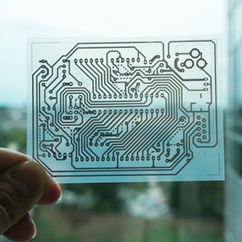 ” Their results will potentially be of use in applications based on the actuation of dynamic 3D printed microstructures such as deformable optics and supporting structural elements for tissue engineering.
Integrating microscopic components into photonic and MEMS systems is one of today's challenges in microdevice manufacturing. Along with this miniaturization, more and more functional components must be placed in ever smaller spaces. Solving this problem using advanced 3D micromachining will pave the way for commercial applications through high-speed data transmission and telecommunications for mobile devices and healthcare. (Source: Nanoscribe)
Source: http://www.photonicsviews.com/on-chip-3d-microprinting-for-photonic-and-mems-systems/
3D printing in electronics
A 3D printer is undoubtedly an excellent device that has become indispensable for many . But often people go too far in their search for new applications for 3D printing. Let's touch on the topic of production of printed circuit boards and REA cases using 3D printers today.
To begin with, let's consider all the methods for creating printed circuit boards (hereinafter PCB).
PCB production
Radio electronics enthusiasts often dream of some kind of device for the production of printed circuit boards at home. Of course, there is the great “LUT” technology (laser ironing technology), as well as the classic photoresist. But often too lazy to mess around with all this, I want someone to do everything for you.
And there are several ways to create PCB:
- Removing the conductive layer. Milling or scraping the copper layer of fiberglass
- Removing the protective layer from the surface of fiberglass
- Illumination of the photoresist
- Applying a protective layer to the fiberglass
- Direct printing of conductive and dielectric tracks on the surface of various materials
- Filling cavities with conductive material Removing the conductive layer Milling or scraping the copper layer of fiberglass
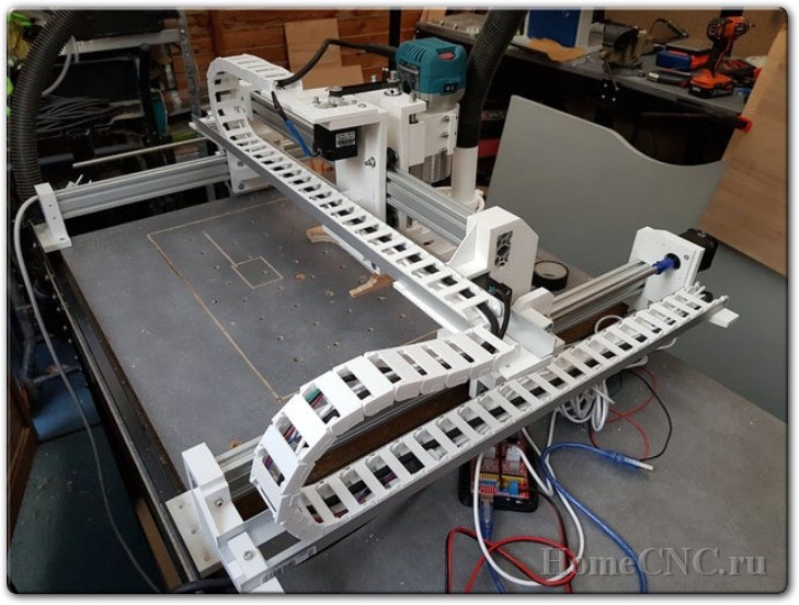
This method is the simplest, and even with a very flimsy and cheap router to cope with this task. Many enthusiasts even put a small engraver on their 3D printers and successfully mill PCB. (Looking ahead, let's say that a 3D printer-based router is only capable of milling PCB, nothing more. A router and a 3D printer are different devices, although many manufacturers try to combine them).
Roland EGX-350
Working area: 305 x 230 x 40 mm; Spindle power: 50W, 20000 rpm; Number of axes: 3
The EGX-350 is the most popular of Roland's engraving machines. With its compact size, complete non-ferrous metal engraving capability, high-speed spindle up to 20,000 rpm, and curved surface engraving, the EGX-350 finds applications in a variety of applications from printing plates, promotional merchandise engraving, creation of wax master models in jewelry, to such engineering applications as marking, engraving of printed circuit boards and electrodes for electroerosion and much more.
Roland EGX-400
Working area: 407 x 305 x 42.5 mm; Spindle power: 72 W, 30000 rpm; Number of axes: 3
The EGX-400 is Roland's professional engraving machine designed specifically for high-speed engraving. With a high-speed spindle up to 30,000 RPM, servo motors in all axes, and FFP (Feed Forward Processing) technology that scans the program several steps ahead and achieves high speed and smooth movement in curves, the Roland EGX-400 is a leader in its class
Roland EGX-600
Working area: 610 x 407 x 42.5 mm; Spindle power: 70W, 30000 rpm; Number of axes: 3
The EGX-600 is Roland's CAMM-2 PRO series of powerful and high precision servo engraving machines for professional 2D/3D engraving and milling at an affordable price. EGX PRO is a series of engraving machines equipped with advanced industrial technology with the power, table size and speed of professional engraving machines, but at affordable prices. The EGX-600 is equipped with a 70W spindle and 30,000 rpm. The EGX-600 is ideal for making high precision embossing dies. In addition, the machines engrave nameplates, tags, medallions, 3D inscriptions, dashboards, printed circuit boards and more.
The machines are not the cheapest and few radio amateurs can afford them. But still, the instructions for preparing the circuit for milling in this article: “A printed circuit board at home, or how to make a printed circuit board at home using a CNC machine.”
This method is not limited to one router, you can also use a sufficiently powerful laser to burn the tracks, or scratch the tracks with a needle. And also use the method of electroerosion.
Laser engraved PP
The last method is rather controversial and is more suitable for the next method.
Removing the protective layer from the surface of fiberglass
Just the method of removing paint with a needle is demonstrated in this video:
A permanent marker is used as a protective layer, and the machine itself is nothing more than a 3D printer.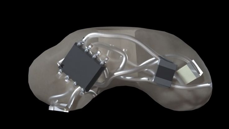
In the same way, any laser module can be used to burn through the upper protective layer, followed by etching.
Illumination of photoresist
It would seem that this method has been known for a long time and what can be invented new? But here, any CNC device comes to our aid. After all, a laser can not only burn a board or a protective layer, but also illuminate the necessary sections of our board with a photoresist. Here are some examples of projects:
LaserExposer - a laser scan from the printer is used to obtain an image. with just a little magic, you can make a good photopolymer 3D printer out of this device.
DiyouPCB - in this case, mechanics and electronics are simpler. But the same principle is used. The laser diode is taken from the BlueRay drive head.
Applying a protective layer on fiberglass
This method can be called one of the simplest, instead of an engraver, laser or print head, we attach a regular permanent marker and draw our board.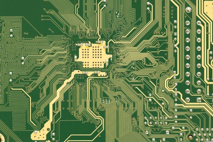 Despite the simplicity in this way it is very difficult to breed a board with thin tracks, the only limitation is the thickness of the marker rod.
Don't forget about our old friend, the regular inkjet paper printer, many convert old technology to print on T-shirts or printed circuit boards. Read more in the article ”Direct Inkjet Printing of PCB Pattern”.
Direct printing of conductive and dielectric tracks on the surface of various materials
The method closest to the topic of 3D printing for creating PCBs and, in some cases, even housings. Let's start with the simplest devices:
Drawing on the textolite surface allows not only applying a protective layer, but also “printing out” a conductive one.
As you know, graphite is a conductor, which allows you to draw a printed circuit board on a sheet of paper. Yes, graphite is not the best conductor and almost certainly such a board will not work, but a pencil can be replaced with a marker with silver ink, as was implemented in the Ex1 PCB
printer. And coming very close to 3D printers, we want to present you two similar projects:
Voltera: Your Circuit Board Prototyping Machine is a device that can print with conductive paste or apply solder for oven baking.
Voxel8 - this device uses the same principle of applying conductors, but immediately prints the body around them. It looks like an integrated circuit. The company demonstrated the potential of this technology using the example of printing a small quadcopter. Undoubtedly, this approach can open up new horizons for creating complex multidimensional circuits and entire devices, but so far this technique has a number of limitations. For example, a fairly large installation and thick, voluminous tracks, you can not use a soldering iron.
By the way, do not discount conductive plastics, and on a two-nozzle printer it is quite possible to print plastic circuits that are quite suitable for training.
Filling cavities with conductive material
And the last method, slightly clumsy, but it has its place. It does not allow to obtain thin and compact boards, or multilayer ones. And also completely eliminates the effects of high temperatures, they can not be soldered.
As you can see, a cheap home printer can be quite successfully used to make PCB, converting it into an engraver (laser or milling), or directly print boards with plastic or paste. It is worth paying your attention to the fact that all of the above methods do not allow the full production of multilayer PCBs, which is a stumbling block for many radio amateurs. We hope that this problem will be successfully solved soon.
Well, the use of 3D printers doesn't end there.
Electronic equipment housings
If everything is less clear with the PP, and even without sophisticated devices for automatically creating circuit boards, you can always return to LUT. That with cases for devices often there are problems.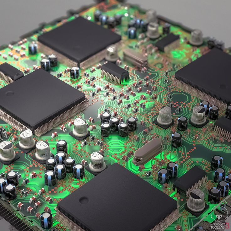 Of course, there are standard REA cases, but they are far from always suitable for homemade products, they require strict adherence to the size of the board and elements, which is not always convenient. Also, do not forget about the aesthetic side of the issue. In this case, a regular FDM 3D printer helps us perfectly. The only question is whether any printer is suitable for these tasks.
Agree, high-quality printing of such complex engineering parts without soluble support is almost impossible.
Large range of business card holders, which can also be successfully used as a “third hand” for wires. As you can see, 3D printers are not limited to CEA housings.
For vaping enthusiasts, a 3d printer can also be useful when designing homemade box mods.
Also, do not forget about housing elements such as latches, thin baffles, etc. These elements, even perfect FDM printers, do not print perfectly, and they cannot withstand the loads that molded parts can withstand. In this case, SLA printers save the situation, for example, the well-known Form 2. And using burn-out photopolymers, you can cast the body of your product from metal (even precious).
In this picture, on the right, the original part from logitech headphones, as we can see, just thin latches are broken. This do was scanned and printed on a Formlabs Form2 3D printer.
Do not forget that the products printed on the Formlabs Form2 photopolymer printer require almost no post-processing, you immediately get a product of unsurpassed quality. This printer allows you to create a master model for casting cases without additional processing, as an example, the case printed by us in maximum detail:
Subsequently cast in silicone:
And a few more cases. Without knowing in advance, few people will distinguish these products from the factory ones.
It is also worth noting that there are different polymers that differ in physical, chemical and optical properties.