3D printer circuits
3D-printed circuit boards: How they're made and why they matter
Once confined mainly to home-brew tinkering, circuit boards created via 3D printing are now practical for some manufactured products.
J.F. Brandon, BotFactory Inc.
In the past ten years, 3D Printing has gone from a niche prototyping tool to a process acceptable for mass production. Most of the recent hubbub has been about monolithic plastic and metals. But new materials and processes have appeared to help create 3D-printed PCBs that meet long-standing engineering problems.
If the history of electronics manufacturing could be summarized in one phase, it would be, “Shrinking everything to nothing to squeeze out something faster.” The push towards miniaturization has been driven by the inviolable laws of nature – faster devices that consume less power require shorter electrical paths.
However, the printed circuit board is an outlier in the electronics world. PCBs still use basic drilling and plating processes perfected 50 years ago. That is not to say that PCB manufacturing is trivial or antiquated. But the investment in new PCB manufacturing methods is a pittance compared to the hundreds of billions put into chip fabs by IC makers such as TMSC and AMD.
It is worth looking at the details of PCBs and their construction. The word ‘printed’ in printed-circuit board only describes half of the process – the silkscreen masks are the only part that is printed. A PCB is originally copper foil on a rigid fiberglass laminate which is selectively etched, drilled, and plated using a set of silkscreens and chemical baths to produce the final product.
Examples of inkjet-printed circuitry made with a BotFactory SV2 PCB printer.The sole purpose of the PCB is to reliably connect passive and active components and provide a reliable platform for integration or interactions with the rest of a product. For example, the PCB in the average computer keyboard connects electronic elements together, but it also must manage human interactions and provide a sound mechanical connection to the body of the product. In addition, PCBs must be designed so they can easily be stenciled with reflow solder paste and integrated into industrial surface-mount pick-and-place lines. Optical inspection and flying-probe systems require PCBs that can be easily analyzed and binned for repair or discard automatically. All in all, modern PCBs can play a variety of roles within the end products in which they are found. So it is worth considering new manufacturing processes that can expand the capabilities of PCBs.
PCBs have thermal, electrical, geometric and mechanical requirements that go beyond what most materials for 3D printing can offer. For example, the average $500 3D printer that uses Fused Deposition Modeling (FDM) uses PLA, ABS and PETG which melt under the harsh gaze of any standard soldering station. Metal 3D printing techniques are designed to handle one material at one time. Yet PCBs require, at a bare minimum, a dense and conductive metal for conductors.
Three technical paths have appeared for PCB printing: inkjets, extrusion, and additive manufacturing (AM)-electroless plating. First consider ink-jetting. New nanoparticle and particle-free inks have allowed inkjet printing to go beyond CMYK inks and graphics. Inkjets can now lay down metal (overwhelmingly silver) inks in fine patterns on flexible materials. In combination with a polymer ink, it is possible to create PCBs with complex multilayer circuitry (blind and buried vias are trivial items) in only a few steps on a single machine.
The inherent advantage of creating PCBs layer-by-layer this way is that each layer can be tested and validated. The minimal level of processing simplifies the dispensing solder paste, part assembly, and testing for every layer. The disadvantages are that material dispensing via inkjet printing is slow relative to all other additive manufacturing processes– deposition speeds can be in the millimeters-per-hour range. It’s possible to create precise traces with inkjet printing (metal traces with 100-micron widths are commonly attainable). But the smaller droplets limit deposition speeds.
And there are problems with metal inks: Applying too much can cause bleeding and cracking during drying, thus limiting PCB fabrication speeds. Solderability is a particular blind spot – silver can wilt under standard pastes like SAC305, suffering from tin ‘scavenging’ silver during reflow. In addition, inkjet polymers melt at temperatures that standard PCBs easily manage. Fortunately, industry-accepted low-temperature tin-bismuth and indium-based solder pastes are compatible with inkjet-printed PCBs.
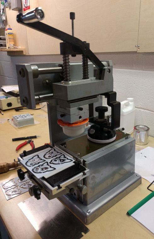
Today there are two PCB printers that use ink jetting – the BotFactory SV2 and the Nano Dimension DragonFly. Each printer uses the same process to create multilayer circuitry, although the BotFactory SV2 utilizes inexpensive thermal inkjet heads instead of the piezo heads found in the DragonFly. Nano Dimension has focused on printing for production, whereas BotFactory has emphasized integration of pasting and PCB assembly into a small unit, working on projects with the USAF to automate the entire process. In this regard, BotFactory is unique in the electronics industry and is the only commercial product below $20,000.
Single nozzle jetting
Inkjetting isn’t the only way that nanoparticles can be deposited to create circuitry. An alternative method extrudes lines onto flat surfaces and uses fused-deposition modeling to provide a polymer structure for the traces to inhabit. Pastes are notoriously difficult to control when creating fine traces and spaces, requiring precise control and extremely close contact with the substrate surface.
Here the target surface must be covered twice – first for mapping, then for pasting. The two-step procedure handicaps the scalability of the process for production. Pastes must be devoid of air pockets lest each bubble act as a kind of ‘spring’ and impede the extrusion process. The flip side of using viscous pastes is that metal-loading is higher and it’s possible to deposit metal in thicker layers, boosting conductivity and solderability right off the bat. However, at this time, silver is the overwhelming favorite material and thus suffers from the same constraints as inkjet-printed PCBs in regards to silver scavenging.
The first example of 3D printed electronics was demonstrated by Voxel8 in 2015. The printer used FDM and paste extrusion to create basic circuit traces. After delivering early beta systems, Voxel8 switched to industrial-scale fabrication with a broader focus on multi-material printing rather than just electronics. nScrypt has taken a similar tack, creating a more general tool that includes pasting as well as polymer extrusion to create three-dimensional objects with traces within the object.
Example of an nScrypt system extruding conductive traces on an FDM-printed substrate.AM + electroless plating (also abbreviated as AMEP, or 3D-Print-and-Plate) is a completely new category of AM that combines existing additive manufacturing processes and well-understood electroless plating techniques. An object is printed via stereolithography (SLA) or fused-deposition modeling (FDM) using a distinct metal-loaded material that can be electroless-plated afterward. AMEP continues to be a topic of academic research. Last year, researchers at UCLA published results on using SLA to create multi-material prints that could be selectively plated. Using two vats of pure and metal-loaded polymers, the process enhances the existing premise of AM with no extra constraint on fabrication speed.
Palladium, a metal that is traditionally extremely expensive, normally serves as a seed material in this process. But on the other side of the world, UK researchers devised a way of printing less expensive metal on a new polyimide material. Polyimide (also known as Kapton) is highly prized by electrical engineers in flexible and printed electronics for its low thermal expansion and dielectric constant. UK researchers found UV energy can be used to chemically bond silver particles and the polymer chains, providing seeds for plating afterward.
The technology described above has not been commercialized, but the overall concept has been utilized for creating unique antennae at firms like Swissto12.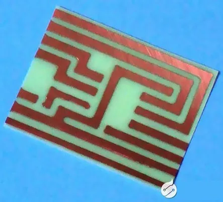 There a high-resolution SLA print is made, coated, and then electro-plated (not electroless plated). Electroplating requires a current to initiate and control the plating process, whereas a PCB often has unconnected traces and vias that require plating.
Overall, the greatest challenge to AMEP is that it cannot create conductors within an object unless there are exposed holes or the PCB undergoes multiple dips into the plating baths. As it stands, the technology has the ability to meet all the technical requirements for high-performance PCBs, including ease-of-solderability and high-thermal tolerances.
What it’s not
There is some confusion about what is and isn’t ‘AM electronics,’ and certain lines have been drawn. In the AM industry overall, any process that uses subtractive processes is not additive manufacturing. So it is fair to argue that any process that builds circuitry on pre-existing substrates or augments AM with subtractive processes is not 3D-printed electronics. Consider the traditional PCB: UV-curable polymers mask copper foils, utilizing a process and materials seen in AM technologies like inkjet printing and stereolithography. By conveniently ignoring the drilling process for vias and shaping, one could argue that PCBs are made with AM when they clearly are not.
When an entire model is fabricated using AM, it typically has characteristics and form factors that go beyond what would be possible if subtractive fabrication is included. In other words, use of subtractive processes detracts from the entire point of adopting AM.
An example of a semi-additive process that is commonly cited as 3D-printed electronics is Laser Directed Structuring, a technique developed by LPKF. Essentially, an object consists of an injection-molded plastic that has been filled or coated by an organometallic compound. When a laser applies a circuit pattern to the surface, metallic seeds form and create an electroless nickel or copper plating. The technology is limited by the reach of the laser, inhibiting the possibility of allowing conductors to pass thru the object. Thus LDS parts are not true 3D PCBs by any means.
The same limitation also applies to aerosol jetting, a concept commercialized by Optomec. Here a carrier gas (nitrogen typically) jets out of a fine nozzle at high speed and carries a fine suspension of materials such as nanoparticle metal inks. The wide variety of viscosity, metal-loading and material choice makes aerosol jetting a candidate for creating sensors on objects, overcoming the limited choice of materials for LDS. As both processes utilize non-AM elements, they arguably do not create 3D-printed electronic devices.
Credible advances in materials, metals and polymers have made it possible to 3D-print PCBs that are useful in many applications today. However, the 3D-printed circuit board made in a few hours which is a perfect replica of a traditional PCB is the Mount Everest of AM. The most mature technique is inkjet printing; it comes closest to reaching the necessary geometric and electric properties, with materials advancing quickly to meet the thermal and mechanical needs. Extrusion is well-understood but hard to scale, and its fundamental capabilities are uneven. AM-EP is the dark horse in the race, combining old and new techniques to provide another path to the 3D PCB.
Ultimately, all technologies can be viable paths to reducing PCB size and shortening traces, yielding lighter devices in forms that would have been unthinkable just ten years ago.
BotFactory Inc.
www.botfactory.co/
What's Possible Now and in the Future?
Ziv Cohen
Application Manager, Nano Dimension
The semiconductor industry gets a lot of attention—and for good reason. Integrated circuits make technology possible, and these devices are built on the back of semiconductors.
Semiconductor manufacturing processes have come a long way since Robert Noyce invented the integrated circuit in 1959. With the rise of Industry 4. 0 and the wide array of additive manufacturing processes, one naturally wonders whether the electronics industry will advance to 3D printing integrated circuits at full scale.
In this discussion, the question naturally arises: Why use additive manufacturing processes to produce integrated circuits? 3D printing is already being used to produce fully-functional PCBs with unique geometry, interconnect architecture, and various levels of component embedding. The ability to 3D print integrated circuits and other semiconductor devices directly into a PCB allows low-volume fabrication of highly specialized devices with unique form factor and capabilities.
IC dies on a silicon wafer
The Current State of 3D Printing Integrated Circuits
Silicon, III-V, and II-VI semiconductor manufacturing processes are highly advanced and are used to produce integrated circuits with less than 10 nm gate sizes. Currently, the most advanced 3D printing processes provide near micron-level resolution and co-deposition of multiple materials.
Co-deposition is critical for 3D printing integrated circuits because conductors and semiconducting materials must be printed simultaneously. The resolution of the most advanced 3D printing systems must still improve before VLSI is possible. In addition to improving device performance, miniaturization will provide much lower power consumption for switching logic gates.
As an example of what is currently possible with 3D printing integrated circuits, researchers at the Air Force Research Laboratory and American Semiconductor recently 3D printed microcontroller SoCs from polymers on a flexible silicon substrate. These microcontroller units offer 7000x memory compared to other flexible integrated circuits at the time. Some envisioned applications include environmental or strain sensing, as well as munitions inventory monitoring.
A flexible microcontroller integrated circuit. This circuit was fabricated using polymers on silicon.
Currently, thin-film transistors (TFTs), diodes, LEDs, can be 3D printed from organic polymers with commercially available and experimental systems. The 3D-printed TFTs can have various contact/gate configurations and can easily be scaled horizontally and vertically. Polymers can be easily doped and functionalized, allowing their electronic and optical properties to be tuned to meet the demands of different devices.
Using polymers on a semiconductor wafer is a natural route to pursue 3D printing integrated circuits. Electrical contacts can already be deposited in an additive manner through a mask (i.e., thermal evaporation, PVD, or CVD), followed by deposition of semiconducting polymers and larger conductive tracks with a 3D printer. Their adaptability to low-temperature processes also makes them ideal for 3D printing integrated circuits directly on standard semiconductor wafers.
Other researchers are working on advancing additive manufacturing processes and materials to enable 3D printing integrated circuits. As an example, the University of Hamburg and Deutsches Elektronen-Synchrotron developed a 3D printing process that can enable the fabrication of integrated circuits. This process uses a mesh of ~20 nm silver nanowires as conductive elements and a thin film of polymer as an insulator or semiconducting material. This process is still in the research phase, but it illustrates how unique nanostructures can be used to fabricate semiconductor devices that rival silicon integrated circuits.
The Economics of 3D Printing Integrated Circuits
In any manufacturing process, the cost structure involved in manufacturing is an important driver of the price of a finished device. Integrated circuits succeed or fail based on the cost of the die on the wafer—when more dies can be placed on a single wafer, the costs per device decreases. The cost structure of integrated circuit manufacturing is responsible for the high costs of highly specialized, low-volume integrated circuits. An excellent example can be found in the defense industry, where the cost of a single FPGA for a complex system can reach tens of thousands of dollars.
The unique cost structure of 3D printed devices changes this economic dynamic. 3D printed integrated circuits do not need to be produced on a wafer and can even be manufactured individually. Because 3D printed devices can be produced with predictable fabrication time, and the cost structure is complexity agnostic, the costs involved in 3D printing electronics depends on the weight of the materials used. This makes 3D-printed integrated circuits highly cost competitive for low-volume production compared to devices produced on semiconductor wafers with standard processes.
Challenges in 3D Printing Integrated Circuits
Commercially available printers are becoming more advanced, and the range of materials useful with these systems is expanding. That being said, there are still some challenges in 3D printing integrated circuits with the same level of performance as integrated circuits on monolithic circuits. These challenges involve finding rigid semiconducting materials that can be adapted to a standard 3D printing process, optimizing these materials for different frequency bands, and bringing printing resolution closer to the nanometer level.
A lithographic process may aid in 3D printing integrated circuits with less than one-micron resolution.
The fact losses and parasitics can be optimized in a variety of polymers for specific frequency bands allows these materials to compete with GaN, which is currently the best option for fabricating RF integrated circuits and SoCs. GaN is currently used in the best SoCs for high-frequency radar modules, as well as in power amplifiers for microwave and mmWave signal chains. Polymers are already used to 3D print substrates for building flexible and nonplanar PCBs, so it is natural to extend these materials to integrated circuits and other semiconductor devices.
To increase the printing resolution, the additive manufacturing industry may need to devise a completely new printing process. Currently, inkjet 3D printing provides among the highest resolution features for 3D printing PCBs, but it remains to be seen if this process can be improved to provide resolution less than 1 micron. The future of 3D printing integrated circuits will likely adapt a photolithography process or functional self-assembly process to produce integrated circuits with competitive resolution.
Innovative companies that are interested in 3D printing integrated circuits and fully-functional PCBs need an additive manufacturing system designed for full-scale production of complex electronics. The DragonFly LDM system from Nano Dimension is ideal for in-house full-scale PCB fabrication of complex electronics with a planar or non-planar architecture. Designers can embed standard components and can experiment with 3D-printed integrated circuits. Read a case study or contact us today to learn more about the DragonFly LDM system.
3d printing | 3D printing applications
Ziv Cohen
Application Manager, Nano Dimension
Ziv Cohen has both an MBA and a bachelor’s degree in physics and engineering from Ben Gurion University, as well as more than 20 years of experience in increasingly responsible roles within R&D.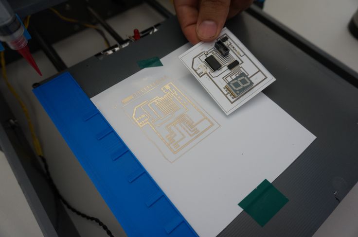 In his latest position, he was part of Mantis Vision team—offering advanced 3D Content Capture and Sharing technologies for 3D platforms. The experience that he brings with him is extensive and varied in fields such as satellites, 3D, electronic engineering, and cellular communications. As our Application Manager, he’ll be ensuring the objectives of our customers and creating new technology to prototype and manufacture your PCBs.
3D printer models
Looking for 3D printer models? The Internet is filled with sites that offer them for free. We have collected the TOP 10 catalogs that you can use to search and download free models in STL format. We hope you can find what you are looking for.
- Yeggi
- Yobi 3D
- STLfinder
→ myminifactory.com
My Mini Factory is a 3D model depository operated by iMakr, an online store that sells 3D printers and accessories. It also has one of the biggest 3D printer shops in Central London. The site contains 3D models designed by professionals, and all models stored on it are checked for quality. You can also make a request for the desired model, which their designers will create and put in the public domain. Billing itself as a 3D printing social network, MyMiniFactory is a thriving community of makers who love to showcase their creations. Users vote for the best models, which allows popular creations to rise to the top of the list and gain popularity. The site presents models that are stored on its social network, as well as outside it, for example, on the Thingiverse and YouMagine sites.
→ thingiverse.com
The most popular and famous site among 3D printer users, Thingiverse is owned by MakerBot Industries, the creator of the popular Replicator 3D printer series. The site allows users to store and share 3D model files that are used with 3D printers. It's a very popular site and has a large community of people hosting various categories of files on it.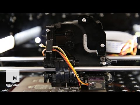 So if you're looking for "cool" printable stuff, Thingiverse is worth a visit. It is a portal designed to provide its users with ways to share their designs and to help print 3D creations. The site has a system that tries to find out what you like. The more you interact with the site, downloading and evaluating various developments, the better its recommendations will be.
→ 3dshook.com
Another online community for 3D printing hobbyists showcasing interesting 3D printer accessories, electronics and most importantly 3D models. The site contains many very interesting models of cars and buildings, as well as various add-ons and spare parts for your 3D printer. A huge catalog of paid and free models for a 3D printer. There are original unique products. Convenient search, navigation, rubricator. 3DShook has over 40 categories and adds over 100 new models to its collection every month. On 3DShook you can always find something for your home, animals, kids or something special for yourself.
→ youmagine.com
YouMagine catalog for Cube series consumer 3D printers manufactured by 3D Systems. The site mainly offers various ways to buy 3D printer supplies and files, but it also has a number of cool free items available, mostly in the Kids section. Some of these elements can be customized by children using an online application. The company offers 3D modeling and publishing tools on its website for both hobbyists and professionals. The site offers a content warehouse where the community hosts and shares models. Registration is required to download files.
→ 123dapp.com
Autodesk 123D is a suite of computer-aided design (CAD) and 3D modeling tools aimed specifically at hobbyists. Along with the toolkit, Autodesk also has a website where users can record their designs and share them with other users. Many of these models can be downloaded and printed using Autodesk as a utility to interface with the MakerBot 3D printer. The goal of the Autodesk website is to "help engineers build products faster." The site offers tools to help them collaborate on their files. For the casual 3D printing enthusiast, the best part of the site is the large library of free files created by a community of over a million engineers. Registration on the site is required, but the number of files that are then available is worth it.
→ cgtrader.com
Being primarily a place to buy and sell a variety of 3D models (not necessarily just those designed for 3D printers), CGTrader does offer a selection of free models that can be used on 3D printers. The site has a system that tries to find out what you like. The more you interact with the site, downloading and evaluating various developments, the body will have better recommendations.
→ cults3d.com
A French community and marketplace where developers can share or sell their creations. The site has a collection of high quality models that you can download.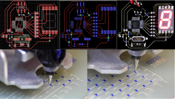 Users can follow the work of the designers they like and get instant updates when a new creation is posted on the site. The site's name, Cults, is a backwards spelling of St. Luc, the patron saint of artists. The site also supports English. This is a relatively new community, so the number of its users is not very large yet.
→ instructables.com
The Instructables website is a community where users can share their DIY projects. This also includes products obtained using 3D printers. The site also provides explanations and instructions describing how to build 3D elements, and some designers take the time to answer questions from site members. Instructables allows users to store and organize their 3D printing projects. This is done to help them work together in the future. You can think of this site as a GitHub 3D printing site where users can share their files, discuss projects, and participate in them. The site also offers the ability to make a request, so if you can't find what you're looking for, you can ask the site's community about it.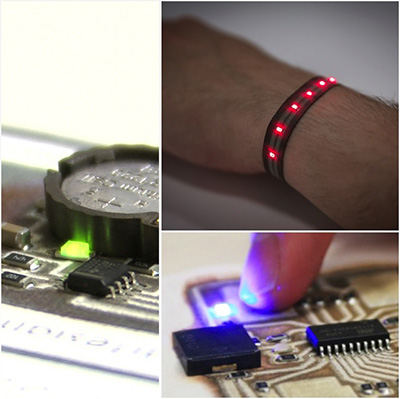
→ pinshape.com
Pinshape, a marketplace for 3D models, is similar in style (layout, look, and ability to capture likes) to the well-known site Pinterest. You can buy models from designers, or download them for printing yourself if they are offered for free. Pinshape allows users to host and share 3D model files on it. Basically, this site acts as an online store where you can buy 3D printed parts, or order your own 3D model to be printed. But if you look closely enough, you can find people who sell their products and also offer the files you need so you can print them yourself.
→ 3dfilemarket.com
A new and growing repository of 3D File Market models. All models are tested for suitability for 3D printing. You can download as many models as you like without registration, although you must provide your email address to access the 3D model files. This is a very simple site aimed at being a repository of model files for 3D printers, and nothing more. The basic design of the site allows users to put files on it for public access, and download files that they would like to use. The site contains many small, simple 3D models ready to be printed, as well as a good selection of everyday items and even spare parts for 3D printers.
Search engines for 3D models in various formats, including STL for a 3D printer. Use queries in English, these search services collect information about models from all over the Internet.
→ yeggi.com
Yeggi is a search engine that will browse major 3D printing sites to find files compatible with 3D printers. You can also browse some popular searches to get an idea of what the community is currently interested in.
→ yobi3d.com
When in doubt, use yobi3D to search for files that match the desired 3D printer. This tool is useful if you want to search for one thing across all sites at once. A very convenient format filter, fast search, high-quality previews and stl models prepared for 3D printing for printing.
→ stlfinder.com
This is another STLfinder that surfs the web looking for 3D printing. To select files compatible with 3D printers, he goes through many 3D modeling sites.
Oops.. there seems to be no such page
Apparently, you've landed on a page that either doesn't exist or was deleted long ago. Start your search first!
Request a call back
Telephone
By clicking on the button, you agree to the privacy policy of
Item added to cart
Go to cart
Product added to comparison
Compare products
Cannot compare more than 4 products
Invoice or quotation request
Organization name:
Your e-mail
Your phone
Name of contact person:
Legal address:
Comment:
By clicking on the button, you agree to the privacy policy of
Goods on the way, find out when delivery
Your name:
Your e-mail
Your phone
By clicking on the button, you agree to the privacy policy of
Contact us
How to call
By phone +7(495)155-45-19. Your call will be answered by an answering machine. We won't call back if you don't speak up. Each request is processed, we contact clients in accordance with requests. Prepare the information you want to report, send it to the answering machine and we will call you back. We kindly request: do not be silent and do not hang up, this is just an answering machine. 🙂 Other most effective ways to get in touch:
- Write to Telegam @techno3dru
- Write to Whatsapp +74951554519
- Write Email [email protected]
Is the product in stock
On the product page, under the product name, there are 3 statuses:
- In Stock - We have this item in stock. Make a purchase with the Buy button.
- Pre-order - goods on the way, delivery soon. Find out about delivery times by clicking on 'Delivery times' or make a purchase using the Buy button.
Learn more