3D printed chips
What's Possible Now and in the Future?
Ziv Cohen
Application Manager, Nano Dimension
The semiconductor industry gets a lot of attention—and for good reason. Integrated circuits make technology possible, and these devices are built on the back of semiconductors.
Semiconductor manufacturing processes have come a long way since Robert Noyce invented the integrated circuit in 1959. With the rise of Industry 4.0 and the wide array of additive manufacturing processes, one naturally wonders whether the electronics industry will advance to 3D printing integrated circuits at full scale.
In this discussion, the question naturally arises: Why use additive manufacturing processes to produce integrated circuits? 3D printing is already being used to produce fully-functional PCBs with unique geometry, interconnect architecture, and various levels of component embedding. The ability to 3D print integrated circuits and other semiconductor devices directly into a PCB allows low-volume fabrication of highly specialized devices with unique form factor and capabilities.
IC dies on a silicon wafer
The Current State of 3D Printing Integrated Circuits
Silicon, III-V, and II-VI semiconductor manufacturing processes are highly advanced and are used to produce integrated circuits with less than 10 nm gate sizes. Currently, the most advanced 3D printing processes provide near micron-level resolution and co-deposition of multiple materials.
Co-deposition is critical for 3D printing integrated circuits because conductors and semiconducting materials must be printed simultaneously. The resolution of the most advanced 3D printing systems must still improve before VLSI is possible. In addition to improving device performance, miniaturization will provide much lower power consumption for switching logic gates.
As an example of what is currently possible with 3D printing integrated circuits, researchers at the Air Force Research Laboratory and American Semiconductor recently 3D printed microcontroller SoCs from polymers on a flexible silicon substrate. These microcontroller units offer 7000x memory compared to other flexible integrated circuits at the time. Some envisioned applications include environmental or strain sensing, as well as munitions inventory monitoring.
A flexible microcontroller integrated circuit. This circuit was fabricated using polymers on silicon.
Currently, thin-film transistors (TFTs), diodes, LEDs, can be 3D printed from organic polymers with commercially available and experimental systems. The 3D-printed TFTs can have various contact/gate configurations and can easily be scaled horizontally and vertically. Polymers can be easily doped and functionalized, allowing their electronic and optical properties to be tuned to meet the demands of different devices.
Using polymers on a semiconductor wafer is a natural route to pursue 3D printing integrated circuits. Electrical contacts can already be deposited in an additive manner through a mask (i.e., thermal evaporation, PVD, or CVD), followed by deposition of semiconducting polymers and larger conductive tracks with a 3D printer. Their adaptability to low-temperature processes also makes them ideal for 3D printing integrated circuits directly on standard semiconductor wafers.
Other researchers are working on advancing additive manufacturing processes and materials to enable 3D printing integrated circuits. As an example, the University of Hamburg and Deutsches Elektronen-Synchrotron developed a 3D printing process that can enable the fabrication of integrated circuits. This process uses a mesh of ~20 nm silver nanowires as conductive elements and a thin film of polymer as an insulator or semiconducting material. This process is still in the research phase, but it illustrates how unique nanostructures can be used to fabricate semiconductor devices that rival silicon integrated circuits.
The Economics of 3D Printing Integrated Circuits
In any manufacturing process, the cost structure involved in manufacturing is an important driver of the price of a finished device. Integrated circuits succeed or fail based on the cost of the die on the wafer—when more dies can be placed on a single wafer, the costs per device decreases. The cost structure of integrated circuit manufacturing is responsible for the high costs of highly specialized, low-volume integrated circuits. An excellent example can be found in the defense industry, where the cost of a single FPGA for a complex system can reach tens of thousands of dollars.
The unique cost structure of 3D printed devices changes this economic dynamic. 3D printed integrated circuits do not need to be produced on a wafer and can even be manufactured individually. Because 3D printed devices can be produced with predictable fabrication time, and the cost structure is complexity agnostic, the costs involved in 3D printing electronics depends on the weight of the materials used. This makes 3D-printed integrated circuits highly cost competitive for low-volume production compared to devices produced on semiconductor wafers with standard processes.
Challenges in 3D Printing Integrated Circuits
Commercially available printers are becoming more advanced, and the range of materials useful with these systems is expanding. That being said, there are still some challenges in 3D printing integrated circuits with the same level of performance as integrated circuits on monolithic circuits. These challenges involve finding rigid semiconducting materials that can be adapted to a standard 3D printing process, optimizing these materials for different frequency bands, and bringing printing resolution closer to the nanometer level.
A lithographic process may aid in 3D printing integrated circuits with less than one-micron resolution.
The fact losses and parasitics can be optimized in a variety of polymers for specific frequency bands allows these materials to compete with GaN, which is currently the best option for fabricating RF integrated circuits and SoCs. GaN is currently used in the best SoCs for high-frequency radar modules, as well as in power amplifiers for microwave and mmWave signal chains. Polymers are already used to 3D print substrates for building flexible and nonplanar PCBs, so it is natural to extend these materials to integrated circuits and other semiconductor devices.
To increase the printing resolution, the additive manufacturing industry may need to devise a completely new printing process. Currently, inkjet 3D printing provides among the highest resolution features for 3D printing PCBs, but it remains to be seen if this process can be improved to provide resolution less than 1 micron.The future of 3D printing integrated circuits will likely adapt a photolithography process or functional self-assembly process to produce integrated circuits with competitive resolution.
Innovative companies that are interested in 3D printing integrated circuits and fully-functional PCBs need an additive manufacturing system designed for full-scale production of complex electronics. The DragonFly LDM system from Nano Dimension is ideal for in-house full-scale PCB fabrication of complex electronics with a planar or non-planar architecture. Designers can embed standard components and can experiment with 3D-printed integrated circuits. Read a case study or contact us today to learn more about the DragonFly LDM system.
3d printing | 3D printing applications
Ziv Cohen
Application Manager, Nano Dimension
Ziv Cohen has both an MBA and a bachelor’s degree in physics and engineering from Ben Gurion University, as well as more than 20 years of experience in increasingly responsible roles within R&D. In his latest position, he was part of Mantis Vision team—offering advanced 3D Content Capture and Sharing technologies for 3D platforms. The experience that he brings with him is extensive and varied in fields such as satellites, 3D, electronic engineering, and cellular communications. As our Application Manager, he’ll be ensuring the objectives of our customers and creating new technology to prototype and manufacture your PCBs.
Interview: A solution to the Semicon chip shortage? How 3D printing is disrupting the $439 billion semiconductor industry
0Shares
Last year, the Semiconductor Industry Association’s (SIA) recorded record sales of $439 billion for the global semiconductor sector. However, the COVID-19 pandemic has cast into sharp relief just how vulnerable global supply chains are, illustrated by a squeeze on the supply of semiconductor chips.
Is 3D printing a solution to enhance supply chain resilience for such a core component of the modern tech world? I spoke with Scott Green, a Principal Solutions Leader at 3D printer OEM 3D Systems, to learn more.
Car manufacturers such as Ford, Toyota, and Nissan have all had to scale back production as silicon microprocessors’ availability has proven to be a manufacturing bottleneck. According to data firm IHS, semicon chip shortages are expected to delay the production of around 1M vehicles in Q1 of 2021 alone. It’s not just the automotive sector either, as games console OEMs like Microsoft and Sony have also experienced severe stock shortages over the past year. The Nintendo Switch drought of early 2020 was a pain point for me, personally.
The DMP 500 Factory 3D printing system. Image via 3D Systems.3D Systems and wafer fabrication tooling
3D Systems’ work in the semiconductor market began when the company acquired Belgium-based LayerWise back in 2014. Before the buyout, the 3D printing service bureau already worked closely with semiconductor companies in and around Eindhoven. The knowledge passed on with the acquisition allowed 3D Systems to establish a semiconductor expertise center in Leuven, where it now works with semicon tooling manufacturers to 3D print optimized wafer fabrication tooling.
Green states, “What’s really interesting for us is to see the uptake in Metal AM components for semicon fab, and to be able to witness the technological advances which affect automotive and smart device manufacturers.”
Wafer fab tooling is the semiconductor industry’s manufacturing equipment, enabling everything from microprocessors to radio frequency amplifiers and LEDs. It encompasses various photolithographic and chemical processing equipment working in tandem, including oxidation apparatus, epitaxial reactors, vapor deposition systems, and etching equipment. Most of the tooling involved in the multi-step process is designed to either deposit or remove materials from a wafer. The process as a whole can take up to 13 weeks, depending on the electronic device manufactured.
Major tooling OEMs such as ASML, KLA, and Lam Research are predominantly involved with highly-specialized parts in low volume. Rather than pumping out as many components as they can, they’re more concerned with refining the quality of their parts and the efficiency of their fabrication processes in a bid to boost productivity and increase yields. For reference, large wafer fab facilities can produce upwards of 100,000 wafers a month, so an increase in productivity of just 5% can result in several thousand extra semicon devices.
Green describes the scenario above as a perfect opportunity for 3D Systems’ Direct Metal Printing (DMP) powder bed fusion technology to lend a helping hand. He explains, “With metal 3D printing, when it comes to producing millions of parts – the cost is too high. We won’t print mountains of mass market heat sinks with low technical requirements, but low-volume, highly complex components and tooling such as semicon fab equipment is a perfect fit. This is a bread and butter DMP application.”
The benefits of DMP 3D printing
Not just an alternative production method, DMP additive manufacturing brings its own set of benefits to the table. First of all, the technology lends itself quite well to geometric optimization, meaning entire assemblies can be consolidated into single lightweight monolithic structures. With free space coming at a premium, this enables overall system complexity to be reduced and mechanisms with printed parts to move faster than their traditionally manufactured counterparts, speeding up the entire wafer fab process.
Green adds, “DMP is probably going to stay a very active topic for semicon tooling companies. You need super clean environments; you need to have the material and end product purity and geometric complexity that our DMP technology offers. Your critical components also need thermal optimization to make sure that you’ve got low thermal gradients and maximum heat dissipation wherever required. .”
.”
As well as enabling performance improvements, DMP can also streamline supply chains. For example, lithography systems are highly complex with hundreds of thousands of parts and complex assemblies. As such, geometric simplification can help bypass the vast supply chain of integrators and subsystem assemblers. Without the need for processes such as braising, welding, fitting, and sheet metal casting, 3D printing wafer fab tooling can potentially drive down manufacturing costs. The technology can also enable faster design iterations in early stage development, as well as faster time to market for semicon systems.
It’s fair to say 3D Systems alone probably isn’t enough to solve our semicon chip shortage, but every little helps when it comes to optimizations in wafer fab tooling. Following the success it has garnered in Europe, the company intends to expand its semicon tooling work to the Bay Area and countries like Japan and Korea, where the most extensive opportunities for process refinement await.
Subscribe to the 3D Printing Industry newsletter for the latest news in additive manufacturing. You can also stay connected by following us on Twitter and liking us on Facebook.
Looking for a career in additive manufacturing? Visit 3D Printing Jobs for a selection of roles in the industry.
Featured image shows the DMP 500 Factory 3D printing system. Image via 3D Systems.
Tags 3D Systems ASML Ford KLA Lam Research Nissan Scott Green Semiconductor Industry Association Toyota
Kubi Sertoglu
Kubi Sertoglu holds a degree in Mechanical Engineering, combining an affinity for writing with a technical background to deliver the latest news and reviews in additive manufacturing.
Live Gambling Casino 3D Printed Poker Chips・Cults
You can play modern poker or roulette with 3D printed casino chips. Read on to find out about these features.
Also known as casino tokens, poker chips are small disc-shaped items used to represent currency in a casino. These chips can be made from plastic, clay, metal, and other materials. Tokens have been used since 1752 when they were used to keep score in card games. Before the game, money is exchanged for casino chips, and after winning, they are exchanged back for money. What's more, chips are a great alternative to money because they look and feel very similar to real coins. You can see how these chips work by playing some casino games on top UK RTP slots.
Once the supplier of these chips is found, the design process begins. Custom chip vendors often offer a variety of samples and templates on their websites to assist customers in the decision making process of making their final custom casino chip. There are many colors and designs to choose from.
After deciding on the design, the material to be used is selected, and there are many materials to choose from, such as plastic, clay, metal, and others. The service provider will then prepare an estimate, and once the final decision is made, payment is made, after which the chips are sent to the place of their use.
Some specific printers are used to print casino chips. Some of the 3D technologies used in printers are as follows:
Stereolithography (SLA)
This type of technology is mainly used to create prototypes and models by layering parts using a photochemical process in which monomers combine to form polymers. It is one of the fastest and most expensive 3D modeling technologies.
3D inkjet materials
This technology is similar to that used in standard inkjet printing. The jets spray droplets of light-sensitive material that harden when exposed to ultraviolet rays. The parts created are designed exactly to the project, and the final product has a smooth surface.
Machines using the above technologies include:
- 1. Ender-3 V2 3D Printer
- 2. Creality Official CR-6 SE by Mech Solutions Ltd.

- 3. Creality 3D Ender-6
- 4. DigiLab 3D45 3D printer
There are a large number of 3D poker chip models on the market today. Here is a list of some of them:
- 1. Chip "Lucky piggy
- 2. Double printed poker chips
- 3. Double extrusion poker chips
- 4. Small blind button for poker chips
- 5. Custom Small Blind Poker Chip
- 6. Poker chip with a bowler hat - depicting the big blind, small blind and dealer chip
- 7. Acrylic poker chips
- 8. Multicolor poker chips
- 9. MTG poker chips
- 10. Lockable poker chips
- 11. Affordable poker chips
- 12. Cryptographic poker chips
- 13. Star Poker Chips
- 14. Lockable poker chips
- 15. Super Smash Bros Poker Chips
- 16. Connectable laser-cut poker chips
- 17. 1830 style poker chips
Poker chips have been around since the dawn of casinos and every modern poker or roulette game needs chips, so why not play with 3D printed casino chips? They are 3D printed and can be any design or texture, and having your own tiles can make the game that much more exciting.
The best part is that you can create your chip online, print it out and have it delivered right to your door!
This page has been translated using machine translation. Suggest the best translation
6 3D printed items that make the best gifts・Cults
When it comes to choosing the right gift, thought matters. But it doesn’t hurt to give something that the recipient will really like. Whether you're looking to try your hand at 3D printing or you're a professional looking for new ways to use your skills, 3D printed gifts are worth checking out.
This can offer a wonderful opportunity for personalization, which psychologists say helps us feel in control. So why not choose a gift that expresses your concern and provides emotional security? (1
So here are six 3D printed gift ideas you should consider.
If you have a friend or family member who loves playing board games or tabletop role playing games (TTRPG), 3D printing can open up a range of cool and unique gift ideas. You can custom make a set of play pieces for their favorite Euro game - something that is sure to spark conversations in your play group in your next session.
If they like to play Dungeons & Dragons or another TTRPG, you can also print 3D dog tags or miniatures. While some people enjoy spending many hours - and many, many dollars - creating and painting miniatures, a 3D printed miniature can make a great gift. Plus, if they like it, you can add to their collection when it's time for the next gift.
If you want to make something truly personal, then 3D printing is the way to go. Personalized items make great gifts because they show that you have thought carefully about what you want to give the gift recipient. Research has shown a wide range of reasons people give for wanting personalized gifts, including everything from the desire for a unique item to self-expression and a sense of ownership. (2)
Whether you're personalizing a bookend set, pencil holder, or cookie cutter, you can include an important date, the recipient's name, or any other detail that will make the gift truly special.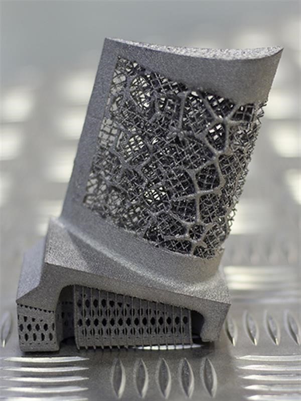
Here's a specific example of a personalized gift that can mean the world to someone, even if it seems small: a personalized keychain. If your friend or family member has a unique name, they may never have the opportunity to buy the kind of souvenir that many people take for granted. You can print their own name keychain for them with a license plate or any other pattern you like and let them know you thought of them and they will carry it around with them.
Sometimes you might have a great gift idea, but the price gets in the way. Let's say your partner loves Star Wars and you know they'll love something lightsaber related, like the special lightsaber featured in the first season of The Mandalorian (no spoilers here). While you might not be able to replicate a glowblade, you can easily find a specific lightsaber hilt design and print it without breaking the bank.
If you want to make a gift inspired by Marvel or DC movies, you can choose your friend's favorite character and 3D print it. Whatever the movie or franchise, there's likely to be a model that fits.
Although this may require a little more skill, for the right person this can be a fun choice. The remote control (RC) model is a great application for 3D printing and can bring endless fun to the recipient, whether it's a child or a hobbyist. If you know someone who is into RC planes, maybe you can help them create the next model. Or, if you have the ability, consider printing an RC car for your niece or nephew, or for your own kids.
This is a fun way to add some style to your desk and give someone something they will use all the time. There are a number of phone cases that can be 3D printed. Plus, you can print a stand for their device so you can easily FaceTime or video chat with them. Even if someone has had the same phone or tablet for years, a new case or stand will make them feel new, all at a great price.
3D printing is interesting because it allows for personalization. If you are thinking about 3D printing a gift for someone, think about their hobbies and what they do every day and you are sure to find something they will appreciate.