3D printing conductive ink
3D Printing PCBs with Conductive Inks: Advantages and Disadvantages
Simon Fried
The number of processes and materials available for use in 3D printing systems for electronic and mechanical products is already extensive, and the options available for product designers is continuously expanding. When it comes to new electronic devices, specifically PCBs, the materials that can be used in any new device depends on the specific additive manufacturing process used for fabrication.
This means that designers need to consider the process they wish to use for fabrication during the design phase, which will also place some limitations on the device architecture. Processes for depositing metals typically proceed at high temperature, or they require the use of a laser to fuse materials into a solid conductive element. These other processes may not be the best option for PCBs, depending on the substrate, desired throughput, and device architecture.
TEM image of gold nanoparticles
As a new class of materials for additive manufacturing of electronics, conductive inks have advantages and disadvantages that need to be considered during the design phase. The mechanical and electrical properties of conductive inks after fusion will affect the range of applications for a finished device. However, conductive inks have simple formulation procedures and are immediately adaptable to existing printing processes, making them an attractive choice for 3D printed electronics.
What Are Conductive Inks for 3D-Printed PCBs?
Conductive ink is simply a suspension of metal nanoparticles in a host liquid. Nanoparticles in solutions can agglomerate over time into larger clusters. Thus, these nanoparticles are conjugated with a ligand to prevent them from clustering in the suspension. The choice of ligand and the host liquid will affect the viscosity of the suspension and its hydrophilicity on a substrate. These points need to be considered when selecting a substrate for use with conductive inks and the appropriate deposition process.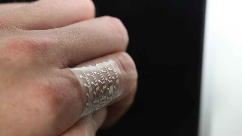
Once this nanoparticle suspension is deposited, the suspending liquid needs to be evaporated and the metal nanoparticles must be fused into a solid conductor. This can involve a high-temperature process, such as annealing, or a lower-temperature process, like optically-assisted sintering and UV exposure. There are other aspects of material selection that should be considered when determining if conductive inks are appropriate for your device and fabrication process.
Conductive Inks Advantages and Disadvantages
The primary advantage of using conductive inks in 3D-printed electronics is their flexibility. They can be deposited on a variety of planar or non-planar substrates. Conductive inks are also adaptable to inkjet printing or aerosol jet printing. The effect on the substrate should be considered when determining whether a conductive ink is appropriate. Ceramic or other rigid substrates can accommodate a higher temperature process without degrading, while a polymer substrate typically requires a lower temperature process.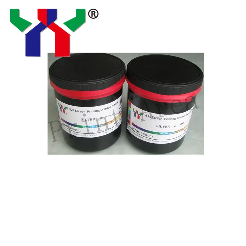
Conductive inks can also be prepared from a wide range of metal nanoparticles. As long as the nanoparticle can be conjugated with an appropriate ligand, the viscosity and hydrophilicity of the ink can be adapted to the deposition process through the use of an appropriate suspending liquid, as well as any additives or surfactants.
Although metal nanoparticles of various shapes and sizes are commercially available, not all additive manufacturing systems are adaptable to all metals, and suppliers of these systems may not provide guidance on how to adapt different metals to their systems. In inkjet printing and aerosol jet printing, the ligand that is used to prevent agglomeration is critical to ensuring the print nozzle does not get clogged during fabrication. At a minimum, the ligand would need to be exchanged prior to deposition, which increases the costs associated with these already expensive materials.
Therefore, systems suppliers spend a considerable amount of time tuning these materials for use with their systems, and it can be difficult for a third party to formulate a new conductive ink for use with these systems. However, the additive manufacturing space is still an emerging area, and the range of available materials is only expected to expand going forward.
One aspect of conductive inks that can be seen as a disadvantage relates to the melting temperature of the metal nanoparticles. The melting point of metal nanoparticles tends to be inversely proportional to the particle size, which needs to be accounted for in the fabrication process. If the processing temperature is too low for a particular conductive ink, then the particles will not fuse into a continuous solid film, and any remaining structural defects in the film can decrease its electrical conductivity and mechanical strength.
Inkjet printing system for use with insulating and conductive inksConductive Inks in Inkjet Printing
The use of conductive inks for inkjet printing is a notable advance in additive manufacturing for electronics. Because the temperature of the fabrication process can be quite low and fusion can be optically-assisted, conductive inks are immediately adaptable for use in inkjet printing systems that can co-deposit conductors and the substrate simultaneously.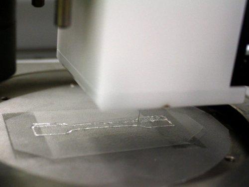 This is a major advantage over other processes like aerosol jet deposition, laser direct structuring (LDS), or fused deposition modeling (FDM).
Simultaneous deposition of conductive ink and a polymer dielectric substrate, followed by simultaneous curing with high-intensity lamps, provides a much higher throughput than aerosol jet deposition, FDM, LDS, or similar processes. This allows a PCB to be deposited in a layer-by-layer process, making inkjet printing a natural choice for fabricating multilayer PCBs with planar or non-planar geometry.
The flexibility offered by inkjet printing and co-deposition of conductive inks and a polymer substrate gives designers significant freedom to create PCBs with unique architectures. Multilayer interconnect geometries are not limited to the traditional trace and vertical via structures used in PCBs on FR4, and conductive components like antennas, sensors, or inductors that can be easily deposited with non-planar geometry. Designers that use this type of system are freed from the constraints imposed by traditional PCB manufacturing processes.
Even though conductive inks have advantages and disadvantages, they are a great material to use for new 3D-printed electronic devices with unique geometries. The DragonFly LDM Lights-Out Digital Manufacturing System from Nano Dimension is uniquely adapted for 3D printing with this material. You’ll have plenty of freedom to design unique devices with planar or non-planar architecture. Read a case study or contact us today if you’re interested in learning more about the DragonFly LDM system.
Conductive Inks
Simon Fried
A co-founder of Nano Dimension, Simon Fried leads Nano Dimension’s USA activities and marketing for this revolutionary additive technology. With experience working in the US, Israel, and throughout Europe, he has held senior and advisory roles in start-ups in the solar power, medical device, and marketing sectors.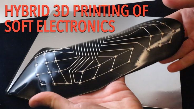 Previously, Simon worked as a consultant on projects covering sales, marketing, and strategy across the automotive, financial, retail, FMCG, pharmaceutical, and telecom industries. He also worked at Oxford University researching investor and consumer risk and decision making.
Conductive Ink | Hackaday
September 14, 2022 by Al Williams
Biological systems often figure out the best ways to get what they need to survive. Now a robot created by researchers at Worcester Polytechnic Institute, Imperial College London, and the University of Illinois Urbana Champaign can make the same claim. The robot operates in front of a plate that has electrical terminals on one end and various obstacles between those terminals and the robot.
The robot can pick up and rearrange some of the items on the plate and then draws paths to the terminals using conductive ink. The effect is the robot gets to “eat” if it solves the connection puzzle.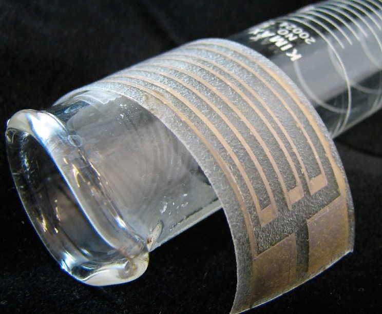
Continue reading “Robot: Will Draw For Food” →
Posted in Robots HacksTagged conductive ink, robotApril 22, 2022 by Anne Ogborn
Surface conductors on vacuum formed parts appear in many hacks, from cosplay armor to 3D touch pads and smart objects. But making them has always been painful. Either they had to be hand painted after forming, which looked sloppy and was labor intensive, or they had to be printed with some difficult to use stretchable ink tech. [Freddie Hong] and his group have another solution, using tech most hackers already have – a 3D printer and a vacuum former.
Smart tray created by this method.They 3D print the traces with conductive PLA filament directly onto a base plastic sheet, and then vacuum form the whole thing. The filament is happy to deform when heated – it’s printer filament.
We like this process. We’ve found conductive filament isn’t reliably resistive across vertical layers, but is reliable in the XY plane.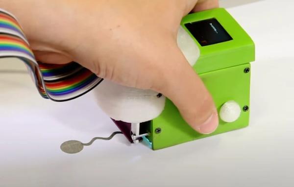 Their method only requires one layer. Also, they suggest 3D printing a layer of non conductive PLA atop most of the conductor, like a PCB solder mask.
Conductive filament has a fair bulk resistance. They suggest electroplating it before applying the top mask layer. They also are exploring 3D printing logos, stripes, and such with colored filament, or even making surface detail like rivets on model parts or adding thickness where the plastic thins during vacuum forming.
Designing the 3D print requires guessing what bit of plastic sheet ends up where in the vacuum formed final part. His group used a commercial program, t-sim, to do the prediction and Grasshopper to import the result into Rhino3D. This seems a lot for a home hacker. Drawing lines on a test sheet and vacuum forming seems simpler.
We’ve looked at vacuum forming before. We did a piece on 3D printing bucks , and covered [Ted Brull]’s Kevo vacuum former back in 2015.
Thanks to [howielowe] for the tip.
February 15, 2022 by Robin Kearey
Although powerful design software and cheap manufacturing services have made rolling your own PCBs easier than ever, there are some situations where a piece of FR-4 just doesn’t cut it: think art projects with hidden LEDs or biomedical applications that need to attach to the human body. For such occasions, [Narjes Pourjafarian] and her team at Saarland University in Germany developed Print-a-Sketch: a handheld device that lets you print electric circuits on almost any surface using conductive ink. Also check out their academic paper (PDF).
The heart of the device is a piezoelectric print head, as used in some types of inkjet printer. It dispenses tiny droplets of silver nanoparticle ink, which is conductive enough to make useful electronic circuits by simply printing a schematic. Lines can be drawn to connect components, while customized footprints can hold LEDs, capacitors or even integrated circuits.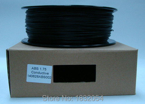
As demonstrated in the video embedded below, the Print-a-Sketch can be used in various different modes. In freehand mode, you can draw whatever you like just by moving the device around. But it also has several assisted sketching modes, where it can straighten out wobbly lines, draw multiple lines in parallel, or even print complete predefined shapes. Especially satisfying is the way it can draw resistors by literally printing zig-zagging lines.
Thanks to an optical motion sensor, similar to the ones used in gaming mice, the device knows at all times where it is and how fast it’s going. That enables the control circuitry to compensate for unsteady movement; the authors claim a printing precision of less than 0.5 mm. In addition, an RGB camera is used to detect the material underneath and adjust the amount of ink dispensed, depending on how absorbent the surface is: rough paper needs more ink to obtain a conductive trace than a ceramic tile.
The number of potential applications seems limitless: how about a yoga mat with integrated touch buttons to control the video player on your iPad? A piece of kinesiology tape with an integrated stretch sensor to measure the exact motion of your arm? Or a floor tile with a printed moisture sensor? All of these are demonstrated by the team, but we’re sure our readers can come up with many more ideas.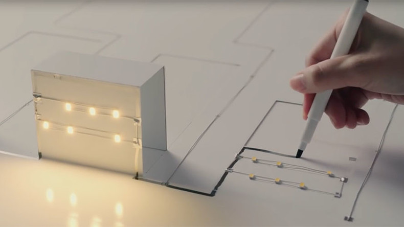
Of course, drawing circuits using conductive ink is not a new idea: previous projects either relied on drawing the entire thing by hand, or used traditional inkjet printers. But the Print-a-Sketch’s sophisticated hardware and software really put it in a league of its own. And since the entire design is open-source, you can simply build one and bring your ideas to life.
Continue reading “Print-a-Sketch Turns Any Surface Into A Printed Circuit Board” →
Posted in Misc HacksTagged conductive ink, handheld printer, printed circuitsFebruary 5, 2021 by Al Williams
Creating your own PC board is a rite of passage for many. These days, though, you can order super inexpensive boards and have them in very little time, so it doesn’t always make sense to build your own. Still, some people like the challenge, and others don’t want to wait even a few days. Probably everyone has dreamed of a 3D printer-like machine that would just crank out beautiful PCBs.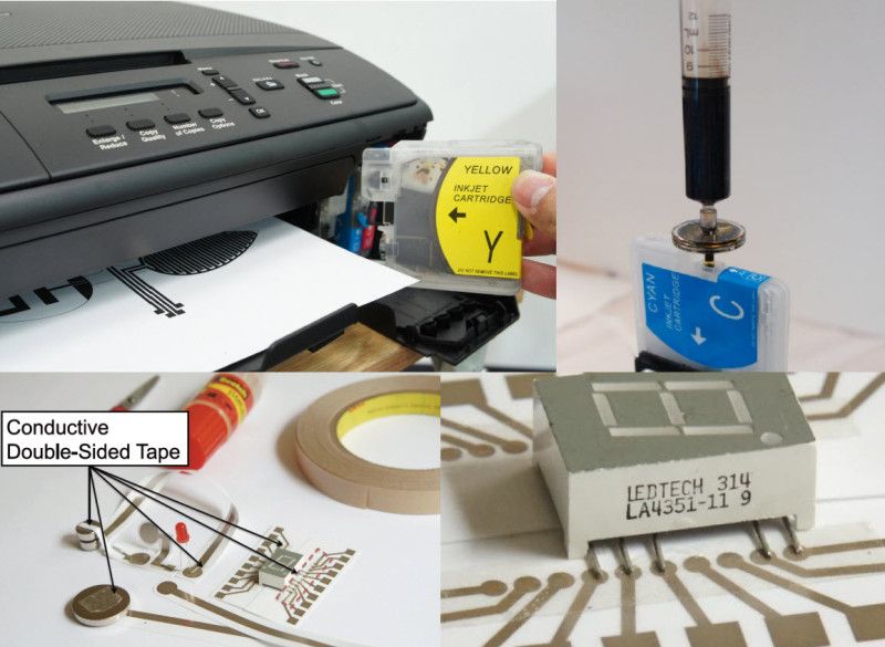 The Voltera V-One isn’t quite at that level of sophistication, but it isn’t too far from it. [Great Scott] shows us how he built two different boards using the system in the video below. While the results were impressive, you can also see that there are several limitations, especially if you are not designing your board with the machine in mind.
One thing that is obvious is that the machine does need your help. In addition to aligning holes, you’ll need to install tiny rivets for vias and slightly less tiny rivets for through-hole components. The last time we looked at the machine, it didn’t do holes at all, but [Scott] shows the drill attachment which allows the machine to produce vias and support leaded components.
Continue reading “Hands On With The Voltera V-One PCB Printer” →
Posted in 3d Printer hacks, Tool HacksTagged conductive ink, pcb, Printed Circuit Board, volteraMay 5, 2018 by James Hobson
If you’ve ever wanted to more fully integrate yourself with technology, you might have to thank a team of researchers — led by [Michael McAlpine] — at the University of Minnesota in the near future. They’ve developed a technique that allows circuits to be printed directly onto your skin, with the team arguing — once the low-cost printer is modified for compact portability — it would be ideal for ‘on-the-fly’ circuit needs.
“But the hand isn’t exactly a stable print bed,” you say. We hear you, and the team is actually one step ahead — the printer can compensate for subtle movements during the printing process by tracking markers placed on the hand. The ‘filament’ is made from silver flakes — akin to conductive ink — which prints and cures at room temperatures, and can be either peeled or washed off. We should hope so, as it’s meant to be layered on human skin.
Speaking of which, it can also print cells!
It’s only been tested on a mouse so far, but the same technology that allows the printer to accurately track the hand means that it could use bio-ink to directly add cells to a wound or some other epidermal affliction to help speed the healing process.
For the circuits, though, you’ll still need the other circuit components and a compact means to power them — to say nothing about the fact that if the circuit is water-soluble, then a little perspiration would cause the ink to run.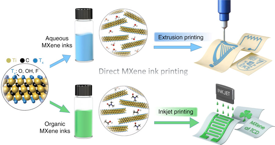 We’re excited to see where this tech goes!
[Thanks for the tip, Qes!]
Continue reading “Printed Circuits In The Palm Of Your Hand” →
Posted in 3d Printer hacks, Wearable HacksTagged bio ink, conductive filament, conductive ink, mobile printing, silver flake, skin cellsApril 13, 2018 by Dan Maloney
The cool kids these days all seem to think we’re on the verge of an AI apocalypse, at least judging by all the virtual ink expended on various theories. But our putative AI overlords will have a hard time taking over the world without being able to build robotic legions to impose their will. That’s why this advance in 3D printing that can incorporate electronic circuits may be a little terrifying, at least to some.
The basic idea that [Florens Wasserfall] and colleagues at the University of Hamburg have come up with is a 3D-printer with a few special modifications. One is a separate extruder than squirts a conductive silver-polymer ink, the other is a simple vacuum tip on the printer extruder for pick and place operations. The bed of the printer also has a tray for storing SMD parts and cameras for the pick-and-place to locate parts and orient them before placing them into the uncured conductive ink traces.
The key to making the hardware work together though is a toolchain that allows circuits to be integrated into the print. It starts with a schematic in Eagle, which joins with the CAD model of the part to be printed in a modified version of Slic3r, the open-source slicing package. Locations for SMD components are defined, traces are routed, and the hybrid printer builds the whole assembly at once. The video below shows it in action, and we’ve got to say it’s pretty slick.
Sure, it’s all academic for now, with simple blinky light circuits and the like. But team this up with something like these PCB motors, and you’ve got the makings of a robotic nightmare. Or not.
Continue reading “Hybrid 3D-Printer Creates Complete Circuits, Case And All” →
Posted in 3d Printer hacksTagged cnc, conductive ink, eagle, fabrication, FDM, g-code, pick and place, slic3r, slicer, smd, vacuumJuly 27, 2017 by John Baichtal
As conductive ink becomes readily available and in greater varieties, we’re starting to see some intriguing applications. [Marion Pinaffo] and [Raphaël Pluviange] created a book of papercraft projects that employ silver-based ink for making a circuit’s wires, carbon-based ink for resistance, as well as color-changing ink. Electronics components’ leads are slipped into slits cut into the paper, connected to conductive-ink traces.
[Marion] and [Raphaël] use 555s, ATtiny85s, watch batteries, and other hardware to make each activity or project unique. A number of projects use a rolling ball bearing to make beeps in a piezo speaker. They also created beautifully designed pages to go with the electronics.
It looks like a fun way for neophytes to play around with electronics, and once the paper part is kaput, the user would be left with the hardware. Imagine one of those beginners googling to find the pinout of the Tiny85 or discovering the Stepped Tone Generator and makes one with the 555.
If you like this project you’ll appreciate the working papercraft organ and papercraft resistor calculator we previously published.
Continue reading “Play With A Papercraft Electronics Activity Book” →
Posted in Misc HacksTagged conductive ink, education, educatonal, papercraftMaterial for 3D printing of "smart" clothes created “Smart” clothes should add some uncharacteristic properties to the item of clothing, so that its usual functions are not violated: wearing, protecting the body from the influence of the external environment, washing. Ideally, it provides non-clothing features such as health monitoring, cold or heat adaptation in addition to traditional functions. Also, such clothing can, for example, collect data and either automatically transmit it wirelessly to an external computer, or process it on its own and then respond to the results of calculations without user intervention.
But first, scientists needed to find a way to cost-effectively print complex, flexible, and durable microchips on a variety of fabrics. Recently, researchers in China have developed a conductive 3D printing ink consisting of droplets of liquid metal coated with alginate, a polymer derived from algae. The scientific article was published in the ACS Applied Materials & Interfaces magazine, and the Nauka TV channel talks briefly about it.
Standard electronics are rigid and cannot withstand the twisting and stretching that clothing is subjected to. Due to their excellent conductivity, gallium-based liquid metals are promising materials for flexible electronics. However, they are difficult to adhere to tissues. Also, the high surface tension causes them to crumple during 3D printing rather than form continuous chains. Zhejiang University has created a new type of conductive ink that can be 3D printed directly onto clothing, creating a variety of patterns.
To make this ink, scientists mixed liquid metals and alginate. Stirring the solution and removing excess liquid led to the formation of microdroplets coated with an alginate microgel shell. The ink was very thick until it was squeezed out through the 3D printing nozzle. This broke the hydrogen bonds in the microgel and made it more fluid. As soon as the ink reaches the surface of the fabric, the hydrogen bonds are restored, so the printed design retains its shape. Alginate ink is removed from clothing by soaking the fabric in a weak sodium hydroxide solution. The liquid metal thus recovered can be used again.
The scientists printed with the new inks on a variety of surfaces, including paper, polyester fabrics, nonwovens, and ribbons on acrylic. The printed circuits had excellent electrical conductivity and deformability. In addition, applying a small voltage to the ends of the circuit caused it to heat up even at low temperatures.
To demonstrate the ink's capabilities, the team printed a series of electronic devices onto commercial clothing. On a T-shirt, they made a short-range communication point that would instruct a nearby smartphone to open a website. Other sensors printed on clothing tracked the movement of the elbow or knee joint.
You can't cry over ink even in February - Nauka - Kommersant
Progress has led to changes in printing methods and opened up new perspectives in the use of printing technologies, which attracts researchers working on the creation of new generation electronics, low cost and the ability to print on substrates large area of various materials.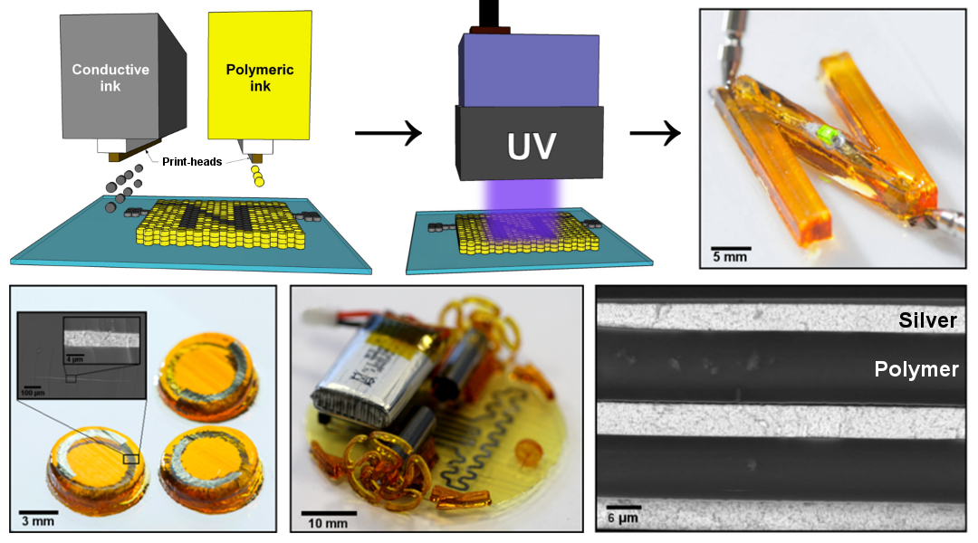 Printing of transistors, capacitors, solar cells and other electronic components is already available. The ink industry has also changed in the last decade.
Types of printing and printing inks
Traditionally, inks are divided into two groups: printing inks (pigment inks) and writing inks (water-based dye solutions). The advantages of ink include low cost, high realism of color reproduction, and the disadvantages are poor light fastness and sensitivity to moisture. Such inks are often used in inkjet printers, where they are used with photographic paper that has a special protective layer against bleeding and discoloration.
Inks are produced for use in various printing methods, which can be roughly divided into conventional printing and so-called non-impact printing. Conventional printing refers to the process of transferring an image or text from a plate to a surface. This can include screen printing techniques (silk-screen printing). Impactless printing creates an image without contact between two surfaces. Examples of impactless printing include laser, thermal, and inkjet technologies.
Functional ink
Structure of graphene ink
Structure of graphene ink
Functional inks are a separate type of printing media that perform a specific function other than color reproduction. These are, for example, luminescent and magnetic ink, which can be used to protect against counterfeiting of documents and banknotes, and even colorless ink based on perovskite nanocrystals for encrypting and decrypting confidential information, developed by scientists from Shanghai University in 2017.
A separate group of functional inks are conductive inks, which have become a natural result of the development of the electronics industry and the desire of electronics manufacturers to miniaturization.
Conductive inks, as their name suggests, act as a conductor of current. In modern inks, metal micro- or nanoparticles (silver, copper, nickel, etc.) are usually used to create electrical conductivity. However, these materials are far from ideal. As a rule, metal nanoparticles have an increased reactivity, as a result of which they are easily oxidized. Metal nanoparticles, as a rule, have a higher percolation threshold, and the cost of their production does not play in their favor.
Graphene inks and their applications
But today conductive inks are experiencing a new round of popularity. This is due to a new modification of carbon - graphene. It is the strongest (200 times stronger than steel) and thinnest material known to mankind. The development of the graphene industry has made the material more accessible for commercial applications. The growing interest in graphene-based conductive inks becomes apparent even after analyzing the publication activity according to the Web of Science platform. If in 2008 there was only one publication with the mention of the term "graphene ink", then in 2018 there are more than 200 such publications. This may also be due to the increase in commercial availability, the emergence of the offer of graphene ink on the market and the ever-increasing and promising potential for the use of graphene in general and graphene inks in particular.
Graphene Ink Experiment Glove
Graphene Ink Experiment Glove
3D printed circuit board printing, smart packaging labeling, electronic textiles, anticorrosive and thermally conductive coatings, RFID tags, flexible polymer electronics, OLED -devices, thin-film photoelectric converters and current sources (supercapacitors and batteries) - this is not a complete list of possible applications of graphene ink. But the greatest return on the use of graphene ink should be expected from areas related to flexible electronics.
In the next 20 years, the global market for flexible electronics will exceed $300 billion. Obviously, flexible electronics will play an important role in solving the key challenges of developing the electronics and systems industry in the coming decades. One of the major challenges in flexible electronics is the development of suitable inks that can be applied using inkjet, screen, flexo or gravure printing techniques to achieve the desired electrical and mechanical performance. The development of technologies for applying graphene from ink to thin substrates opens up wide opportunities for creating thin-layer supercapacitor electrodes, which, as a miniature energy source, attract a lot of attention from developers. Such power sources will be suitable for portable electronics, miniature devices and smart textiles. Therefore, the development and optimization of the technology of mass production of graphene ink are of high relevance for the development of flexible electronics and portable power sources, since the high cost of such materials is currently a constraint for the development of these areas.
“The potential applications of graphene are truly limitless. We have been developing in the graphene industry for ten years now, and we understand this well,” says Sergei Baskakov, General Director of Grafenox LLC.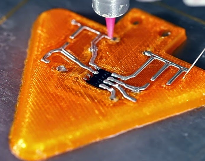 “We have developed several graphene ink formulations for printing conductive coatings both by screen and inkjet printing. Our graphene ink is essentially a suspension of graphene particles in various solvents, including water. In some cases, a binder is added to keep the particles in suspension, which can be easily removed by heating the substrate to low temperatures. Our inks can find applications in field-effect transistors, photodetectors, solar cells, LEDs, electro-optical modulators and many other types of electronic devices.”
“Together with the Laboratory of Polymer Composite Materials NIFKhI them. L. Ya. Karpov, we are performing a series of works on the use of graphene ink in piezosensors based on ferroelectric polymers,” continues Sergey Baskakov. “We are already seeing that the use of graphene leads to an improvement in the characteristics of such devices. Graphene coatings can be successfully used in piezoelectric sensors for biomedical applications (eg, bionic prostheses, artificial muscles).