3D printed circuitry
3D-printed circuit boards: How they're made and why they matter
Once confined mainly to home-brew tinkering, circuit boards created via 3D printing are now practical for some manufactured products.
J.F. Brandon, BotFactory Inc.
In the past ten years, 3D Printing has gone from a niche prototyping tool to a process acceptable for mass production. Most of the recent hubbub has been about monolithic plastic and metals. But new materials and processes have appeared to help create 3D-printed PCBs that meet long-standing engineering problems.
If the history of electronics manufacturing could be summarized in one phase, it would be, “Shrinking everything to nothing to squeeze out something faster.” The push towards miniaturization has been driven by the inviolable laws of nature – faster devices that consume less power require shorter electrical paths.
However, the printed circuit board is an outlier in the electronics world. PCBs still use basic drilling and plating processes perfected 50 years ago. That is not to say that PCB manufacturing is trivial or antiquated. But the investment in new PCB manufacturing methods is a pittance compared to the hundreds of billions put into chip fabs by IC makers such as TMSC and AMD.
It is worth looking at the details of PCBs and their construction. The word ‘printed’ in printed-circuit board only describes half of the process – the silkscreen masks are the only part that is printed. A PCB is originally copper foil on a rigid fiberglass laminate which is selectively etched, drilled, and plated using a set of silkscreens and chemical baths to produce the final product.
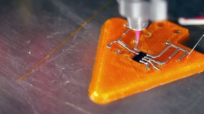
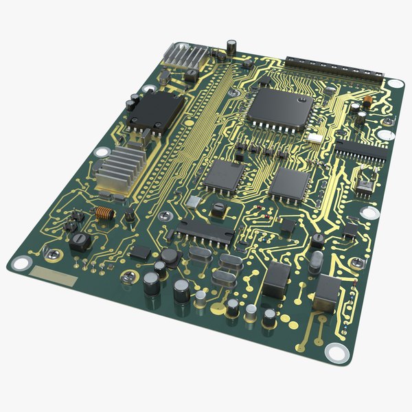
Examples of inkjet-printed circuitry made with a BotFactory SV2 PCB printer.The sole purpose of the PCB is to reliably connect passive and active components and provide a reliable platform for integration or interactions with the rest of a product. For example, the PCB in the average computer keyboard connects electronic elements together, but it also must manage human interactions and provide a sound mechanical connection to the body of the product. In addition, PCBs must be designed so they can easily be stenciled with reflow solder paste and integrated into industrial surface-mount pick-and-place lines. Optical inspection and flying-probe systems require PCBs that can be easily analyzed and binned for repair or discard automatically. All in all, modern PCBs can play a variety of roles within the end products in which they are found. So it is worth considering new manufacturing processes that can expand the capabilities of PCBs.
PCBs have thermal, electrical, geometric and mechanical requirements that go beyond what most materials for 3D printing can offer. For example, the average $500 3D printer that uses Fused Deposition Modeling (FDM) uses PLA, ABS and PETG which melt under the harsh gaze of any standard soldering station. Metal 3D printing techniques are designed to handle one material at one time. Yet PCBs require, at a bare minimum, a dense and conductive metal for conductors.
Three technical paths have appeared for PCB printing: inkjets, extrusion, and additive manufacturing (AM)-electroless plating.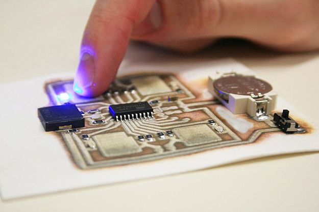 First consider ink-jetting. New nanoparticle and particle-free inks have allowed inkjet printing to go beyond CMYK inks and graphics. Inkjets can now lay down metal (overwhelmingly silver) inks in fine patterns on flexible materials. In combination with a polymer ink, it is possible to create PCBs with complex multilayer circuitry (blind and buried vias are trivial items) in only a few steps on a single machine.
The inherent advantage of creating PCBs layer-by-layer this way is that each layer can be tested and validated. The minimal level of processing simplifies the dispensing solder paste, part assembly, and testing for every layer. The disadvantages are that material dispensing via inkjet printing is slow relative to all other additive manufacturing processes– deposition speeds can be in the millimeters-per-hour range. It’s possible to create precise traces with inkjet printing (metal traces with 100-micron widths are commonly attainable). But the smaller droplets limit deposition speeds.
And there are problems with metal inks: Applying too much can cause bleeding and cracking during drying, thus limiting PCB fabrication speeds. Solderability is a particular blind spot – silver can wilt under standard pastes like SAC305, suffering from tin ‘scavenging’ silver during reflow. In addition, inkjet polymers melt at temperatures that standard PCBs easily manage. Fortunately, industry-accepted low-temperature tin-bismuth and indium-based solder pastes are compatible with inkjet-printed PCBs.
Today there are two PCB printers that use ink jetting – the BotFactory SV2 and the Nano Dimension DragonFly. Each printer uses the same process to create multilayer circuitry, although the BotFactory SV2 utilizes inexpensive thermal inkjet heads instead of the piezo heads found in the DragonFly. Nano Dimension has focused on printing for production, whereas BotFactory has emphasized integration of pasting and PCB assembly into a small unit, working on projects with the USAF to automate the entire process. In this regard, BotFactory is unique in the electronics industry and is the only commercial product below $20,000.
Single nozzle jetting
Inkjetting isn’t the only way that nanoparticles can be deposited to create circuitry. An alternative method extrudes lines onto flat surfaces and uses fused-deposition modeling to provide a polymer structure for the traces to inhabit. Pastes are notoriously difficult to control when creating fine traces and spaces, requiring precise control and extremely close contact with the substrate surface.
Here the target surface must be covered twice – first for mapping, then for pasting. The two-step procedure handicaps the scalability of the process for production. Pastes must be devoid of air pockets lest each bubble act as a kind of ‘spring’ and impede the extrusion process. The flip side of using viscous pastes is that metal-loading is higher and it’s possible to deposit metal in thicker layers, boosting conductivity and solderability right off the bat.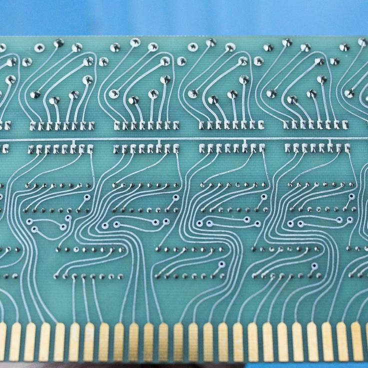 However, at this time, silver is the overwhelming favorite material and thus suffers from the same constraints as inkjet-printed PCBs in regards to silver scavenging.
The first example of 3D printed electronics was demonstrated by Voxel8 in 2015. The printer used FDM and paste extrusion to create basic circuit traces. After delivering early beta systems, Voxel8 switched to industrial-scale fabrication with a broader focus on multi-material printing rather than just electronics. nScrypt has taken a similar tack, creating a more general tool that includes pasting as well as polymer extrusion to create three-dimensional objects with traces within the object.
Example of an nScrypt system extruding conductive traces on an FDM-printed substrate.AM + electroless plating (also abbreviated as AMEP, or 3D-Print-and-Plate) is a completely new category of AM that combines existing additive manufacturing processes and well-understood electroless plating techniques. An object is printed via stereolithography (SLA) or fused-deposition modeling (FDM) using a distinct metal-loaded material that can be electroless-plated afterward. AMEP continues to be a topic of academic research. Last year, researchers at UCLA published results on using SLA to create multi-material prints that could be selectively plated. Using two vats of pure and metal-loaded polymers, the process enhances the existing premise of AM with no extra constraint on fabrication speed.
Palladium, a metal that is traditionally extremely expensive, normally serves as a seed material in this process. But on the other side of the world, UK researchers devised a way of printing less expensive metal on a new polyimide material. Polyimide (also known as Kapton) is highly prized by electrical engineers in flexible and printed electronics for its low thermal expansion and dielectric constant. UK researchers found UV energy can be used to chemically bond silver particles and the polymer chains, providing seeds for plating afterward.
The technology described above has not been commercialized, but the overall concept has been utilized for creating unique antennae at firms like Swissto12. There a high-resolution SLA print is made, coated, and then electro-plated (not electroless plated). Electroplating requires a current to initiate and control the plating process, whereas a PCB often has unconnected traces and vias that require plating.
Overall, the greatest challenge to AMEP is that it cannot create conductors within an object unless there are exposed holes or the PCB undergoes multiple dips into the plating baths. As it stands, the technology has the ability to meet all the technical requirements for high-performance PCBs, including ease-of-solderability and high-thermal tolerances.
What it’s not
There is some confusion about what is and isn’t ‘AM electronics,’ and certain lines have been drawn. In the AM industry overall, any process that uses subtractive processes is not additive manufacturing. So it is fair to argue that any process that builds circuitry on pre-existing substrates or augments AM with subtractive processes is not 3D-printed electronics. Consider the traditional PCB: UV-curable polymers mask copper foils, utilizing a process and materials seen in AM technologies like inkjet printing and stereolithography. By conveniently ignoring the drilling process for vias and shaping, one could argue that PCBs are made with AM when they clearly are not.
When an entire model is fabricated using AM, it typically has characteristics and form factors that go beyond what would be possible if subtractive fabrication is included. In other words, use of subtractive processes detracts from the entire point of adopting AM.
An example of a semi-additive process that is commonly cited as 3D-printed electronics is Laser Directed Structuring, a technique developed by LPKF. Essentially, an object consists of an injection-molded plastic that has been filled or coated by an organometallic compound. When a laser applies a circuit pattern to the surface, metallic seeds form and create an electroless nickel or copper plating. The technology is limited by the reach of the laser, inhibiting the possibility of allowing conductors to pass thru the object. Thus LDS parts are not true 3D PCBs by any means.
The same limitation also applies to aerosol jetting, a concept commercialized by Optomec. Here a carrier gas (nitrogen typically) jets out of a fine nozzle at high speed and carries a fine suspension of materials such as nanoparticle metal inks. The wide variety of viscosity, metal-loading and material choice makes aerosol jetting a candidate for creating sensors on objects, overcoming the limited choice of materials for LDS. As both processes utilize non-AM elements, they arguably do not create 3D-printed electronic devices.
Credible advances in materials, metals and polymers have made it possible to 3D-print PCBs that are useful in many applications today. However, the 3D-printed circuit board made in a few hours which is a perfect replica of a traditional PCB is the Mount Everest of AM. The most mature technique is inkjet printing; it comes closest to reaching the necessary geometric and electric properties, with materials advancing quickly to meet the thermal and mechanical needs. Extrusion is well-understood but hard to scale, and its fundamental capabilities are uneven. AM-EP is the dark horse in the race, combining old and new techniques to provide another path to the 3D PCB.
Ultimately, all technologies can be viable paths to reducing PCB size and shortening traces, yielding lighter devices in forms that would have been unthinkable just ten years ago.
BotFactory Inc.
www.botfactory.co/
A New Way To Produce PCBs With Your 3D Printer
- by: Tom Nardi
With the low-cost PCB fabrication services available to hackers and makers these days, we’ll admit that making your own boards at home doesn’t hold quite the appeal that it did in the past. But even if getting your boards professionally made is cheaper and easier than it ever has been before, at-home production still can’t be beat when you absolutely must have a usable board before the end of the day.
If you find yourself in such a situation, this new method of DIY PCB production detailed by [Adalbert] might be just what you need. This unique approach uses a desktop fused deposition modeling (FDM) 3D printer throughout all of its phases, from creating a stencil based on the exported board design, to warming the UV soldermask to accelerate the curing process. It may not be an ideal choice for densely packed boards with fine-pitch components, but could definitely see it being useful for many prototypes.
Small “bridges” need to be manually added to hold the stencil together.[Adalbert] has done an excellent job of documenting the process through a step-by-step guide posted on Hackaday.io, and has also put together a video you can see after the break.
But if you’re looking for the short version, the process involves taking a 2D DXF from your PCB design software, converting it into three dimensions, and printing it out. This is then placed over a copper clad board that has been coated with soldermask, and a UV light source is used to expose it. Afterwards, isopropyl alcohol can be used to wash away the unexposed mask, leaving behind your PCB design.
You’ll still need to chemically etch the board, and if you’re using through-hole components, manually drill your holes. But compared to some of the old school methods of making your own boards, it’s relatively straightforward. This technique looks like it could also hold promise for small scale production, as the stencil can be reused indefinitely.
If your 3D printer is of the resin variety, don’t worry, you can make PCBs with those as well. We’ve also seen impressive boards produced with cheap laser engravers, as well as budget CNC routers.
The principle of operation of the 3D printer
This is a device that allows you to create three-dimensional objects of varying complexity from consumables.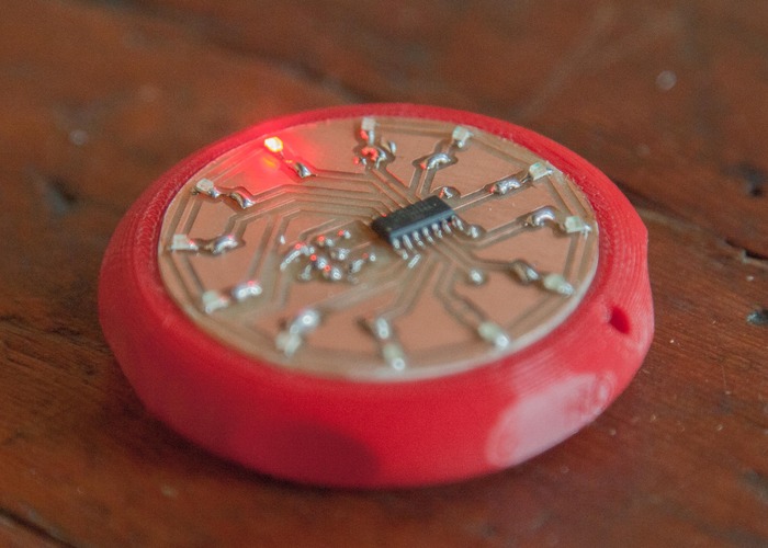 These objects must be modeled in a special CAD program and transferred to print as a file of a certain format.
- Basic principle of operation
- Photopolymer printing
- How a 3D printer works
- How printing works
- 3D printing applications
- Design features of 3D printers
- Layer by layer: how a 3D printer works
Basic principle of operation
- An object is modeled on a computer in a special CAD program;
- the finished object, saved in a special format, is cut by the slicer program that comes with the device, and the thickness of each layer is determined by the capabilities of the 3D printer and the selected settings;
- each layer is translated into a binary command code that the device receives, and in accordance with which, according to the coordinates, a layer of material is applied;
- layer by layer the object is formed.
3D printing technologies
There are quite a number of technologies used in 3D printing. From technology and technology depends on the material used for printing. Currently, for this you can use: plastic threads, photopolymer resins, metal powder alloys; gypsum composite powder, wax, as well as various building and culinary mixtures.
The most famous 3D printing technologies are:
- FDM;
- SLS and SLM;
- lamination;
- photopolymer printing;
- plaster printing;
- construction printing with concrete mix and others.
Fusion Fusion
The simplest and most popular printing technology is FDM or Fusion Fusion.
It involves the supply of a plastic thread to a special heating element.
Using an extruder, molten plastic is deposited in a predetermined printable area. The extruder is fixed on the print head, which moves along the print working area in a horizontal plane. Once the layer has been printed, the work platform will lower by the layer amount and work will continue again.
This type of printing is the most affordable. And devices based on it are the cheapest. That is why such 3D printers are the most popular for home and household purposes, that is, personal use.
Photopolymer printing
Photopolymer printing is a little different. The material is also applied in layers, but it is initially in a liquid state in a special bath. Layer by layer, a laser or ultraviolet beam acts on the material, and the platform rises. That is, the object is, as it were, grown. Under the action of radiation, the material polymerizes and hardens.
Since this technology allows to obtain products with the highest accuracy, including thin-walled ones, it is more promising and has more opportunities. It is used in complex industries and enterprises.
Such devices are also in demand in the medical field, opening up the widest possibilities for manufacturing high-precision surgical templates and even prostheses.
How a 3D Printer Works
The general scheme by which all 3D printers work is based on the ability to move linearly in three dimensions.
The devices are equipped with high-precision stepper motors and a controller responsible for the order of movement of these motors.
Automated system moves the print head to extrude material (such as melted plastic) at the right time.
Layer by layer, a figurine is created that was originally included in the program.
It is based on the principle of the "Cartesian robot" (a device capable of moving along the Cartesian coordinates, better known to every schoolchild as the Cartesian coordinates - X, Y, Z).
Approximate diagram of a 3d printer print head It is this detail that is most often improved in new models and is considered the most complex and subtle part of the movement. It consists of a thermal head and a drive that extrudes a plastic thread. It works like this: a spool of filament is threaded into the printer, the drive unwinds and ejects it, feeding it to the thermal head (also called the camera). The head is usually a heated aluminum element that melts the filament. 3d printer software First, a model of the future object is created using special software, then it is loaded into a printer, which creates a physical object using the technology described above. This method is called prototyping. But now there are several more principles of operation of 3D printers developed on its basis: These are just the basic and most common methods, in fact, there are many more rare, highly specialized options - for example, UV irradiation through a photomask (SGC), layer-by-layer bonding of films, bonding of powders, laminating sheet materials (LOM) and others. The technology has found application in almost all areas of human activity: Chocolate 3d printer pizza printed on 3D printer Matca of the house, printed on 3D printer car, printed on 3D printer The principle of operation of a 3D printer is based on the laws of kinematics. There are several 3D printing schemes based on the movements of the platform and the print head, which can move relative to each other in different planes. There are four main print patterns: The platform is stationary, the position along the x, y, z axes is changed only by the extruder. A feature of the model is the presence of a high frame. The print head is placed on three rods, each of which is fixed on a movable block placed on a support, with the possibility of vertical movement. Pros: high print speed, good accuracy. Loading Delta Loading The extruder moves along the X and Y axes The extruder, as in the previous type, is able to move to the left or right, as well as change its position in space in height. The platform, in turn, is able to move forward or backward without changing its height. Loading The extruder moves along the X and Z axes The latter scheme involves the use of a fixed platform. The most affordable and therefore the most common method of 3D printing, in which the finished object is created from liquid plastic or composite materials that pass through an extruder printhead and are laser-cured layer by layer. The finished layer is shifted down, and a new one is printed, and so on until the entire element is ready. FDM printers are one of the easiest ways to 3D print, and you can even assemble them yourself. Well, or buy ready-made solutions, of which there are many on the market. By its principle of operation, this type of 3D printing is similar to the previous one, only in it the starting material is liquid resin (acrylic, epoxy, vinyl) or plastic. The laser beam "bakes" the source material in layers, forming the finished object. Another method of layer-by-layer printing of objects, in which the laser sinters the powder - metal, plastic or ceramic - layer by layer, forming the finished object. There is a melting technique (SLM), which is distinguished by more powerful lasers and the ability to work with pure metal powder without any additives - this is how monolithic elements are formed, devoid of the porosity characteristic of conventional sintering. As a rule, the thickness of the thread and the layers themselves are fractions of a millimeter: a typical nozzle diameter varies from 0. One of the most attractive features of FDM printing is the huge variety of relatively inexpensive consumables. The two most popular plastics are ABS (Acrylonitrile Butadiene Styrene) and PLA (Polylactide). The first option is familiar to all of us - it is the most widely used industrial plastic, which is made from your favorite coffee grinder, ballpoint pen, smartphone protective cover and many other household items. The second is a sustainable alternative, being an organic, biodegradable polymer made from corn or sugar cane. Although PLA is not so durable, it can be safely thrown into the trash, because under the influence of the environment, after a few months, polylactide will turn into harmless compost. Liked the article? Tell your friends: Rate the article, it is very important for us: Voters: 2 people As a final result, we need to get a gerber file for one layer of copper and, possibly, another layer for a protective solder mask, but why bother with trifles - then also prepare the silkscreen and make a stencil for the paste . It all starts with the component library. Footprints for SMD components do not differ much from those for a multilayer board or a single-sided, more precisely, single-layer, except for different soldering modes - manual, paste, wave, or something else. For home use, manual soldering is more often used or on paste, also manual, i.e. not automated. But with DIP components, things are different, because. there is no plating in the holes, and in order for the platform to hold the component well, its size is increased. Thus, for hand soldering and single-layer boards without hole plating, it is reasonable to make a separate library of components. Yes, and the set of rules will have to be corrected in order not to make paths too thin without urgent need, because. the wider the traces and gaps, the easier it is to control the PCB manufacturing process. Further, the process of designing a printed circuit board is no different from the industrial version. What Delta Design lacks for single layer boards is automatic SMD and/or DIP jumper placement. But even without this, it is possible to design a board, however, it is not very comfortable, if I may say so. When the library is prepared, we start creating the board. Everything is simple here, the main thing is not to forget to immediately indicate the 3rd class of accuracy - it is quite feasible for home production. The board is designed, the only thing left is to upload Gerber files to production . In Delta Design, export to gerbera is called differently: “Create Production Files” There remains one more necessary operation - this is the addition of holes on the apertures of DIP components for subsequent drilling at home - the hole must be smaller than the diameter of the drill, because. it is only needed to guide the drill while drilling the board. To do this, in the aperture editor, find the necessary apertures and change their hole diameter. Further, the ways of manufacturing a printed circuit board may differ. In my example, I will illuminate the photoresist using a UV laser pointer installed on a 3D printer. There is no functionality in DeltaCAM with which you can generate a GCode for execution on a CNC machine, for this stage I use FlatCAM (http://flatcam.org). Details about connecting a laser pointer, GCode preparation described in another article. 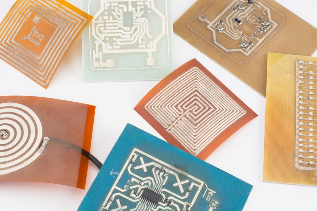 In a semi-liquid state, the substance is squeezed out through the opening of the print head.
 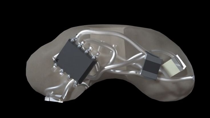 The platform is usually made of aluminum or glass - a substance with good heat conductivity.
 How printing works
 After the layer is formed, the elevator raises or lowers the workpiece.
Applications of 3D printing
0
. printers
I scheme
II scheme - the extruder moves along the X and Y axes
III scheme - the extruder moves along the X and Z axes
IV scheme - the extruder moves along the X, Y and Z axes
 As in the case of the "Delta" scheme, the extruder is able to move along three axes [x, y, z], but in this case there is no complex mechanism for fixing the print head.
 Layer by layer: how a 3D printer works
Stereolithography (SL or SLA)
 It is then rinsed free of resin or plastic residue and subjected to a final curing with ultraviolet light. Stereolithography allows you to print elements with fine detail, and after completing all the procedures, the finished part is strong and chemically resistant, but the reverse side of the coin is the very high cost of such 3D printers.
 Selective Laser Sintering (SLS)
 3 to 0.8 mm, while the thickness of the layer is from 50 to 300 microns. For comparison, the thickness of a human hair ranges from 80-100 microns. Obviously, printing with a thin thread takes quite a long time. Indeed, a typical production cycle can easily be measured in hours or even more than a day: it all depends on the selected nozzle diameter, the thickness of the individual layers and the dimensions of the product itself. The higher the thickness of the thread and layers, the less time it will take to print, but the quality of the surfaces will be lower.
 Consumables

Average rating: 5 out of 5 I'll tell you how you can make a board at home using Delta Design. The order of work is something like this: Delta Design -> DeltaCAM -> FlatCAM -> 3D printer with laser pointer . In my hobby, I periodically need to make prototyping boards to test and / or connect microcircuits with minimal strapping, in this case, an example will be for connecting a MAX5725 DAC.
 .. but that's for another time.
In addition to the rules, you can also choose the format right away, if the scheme is not large, then I choose the A4 format:
Let's move on to creating a circuit and a printed circuit board layout - this is a creative process and everyone does it in their own way. Prepared the circuit and board:
On the DOCUMENTUM layer, I added graphics - text and a circle for later merging on the copper layer along with the PCB layout.
The only thing you need to pay attention to is the choice of grid for the board editor.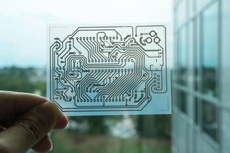 By default, there is only a millimeter grid, but often you have to make boards with pin connectors like PLS. And then I insert such scarves into the circuit board with holes with a pitch of 2.54 mm or connect them with wires with Dupont connectors. So, in order to put the connectors at the right distance, a multiple of 2.54 mm, it would be convenient to switch the grid to this step and arrange the connectors. The grid setup for the board needs to be done in the standards once:
There's a tricky grid setup relative to the base grid:
Added grid 1.27 and 2.54. The mesh can now be toggled in the PCB editor in the lower left corner.
About once, I lied. Delta Design is frequently updated and needs to be reinstalled frequently. Therefore, if you set it up for yourself once, then you need to export the standards to a DDS file and, after the next update, import the standards before starting work with the new version of CAD.  .. But there are also a few points here, which I will dwell on in more detail. For a single-layer board, I usually combine the outline of the board, the copper layer and graphics, for example, put a logo or make inscriptions. In addition, checking the output gerber file in the viewer is also useful.
In the form, select which layers you want to display and indicate that all this should be saved in the project tree. If you need to look at the files in an external viewer, you can choose to save the files to disk.
After creating the production files, a line with the factory icon appears in the project tree:
Open this item and see all the layers that we have selected. This is a DeltaCAM Gerber file viewer and editor already built into Delta Design.
Here you can already transfer the graphics from one layer to another.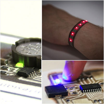 Select the desired layer with graphics, select all the necessary objects and change the layer for them in the properties:
Thus, we transfer everything to the SIGNAL_TOP layer. The peculiarity of this operation is that during such an operation there is no conversion of graphics and objects in the Gerber file. They are simply transferred without changes.
In this example, two apertures are needed for drilling - an oval and a rectangle, DCode 5 and 16, respectively. We make the hole diameter minimal and sufficient for etching at home. This operation also does not change the graphics of the Gerber files, as simply complements the parameters in the description of the aperture according to the Gerber standard. As a result, we immediately see the changes:
The board is now ready for production. We upload the Gerber file of the desired layer and prepare it for making a photomask, a picture for a LUT, or for laser illumination on a home CNC machine, such as a 3D printer. Uploading the edited layer to a file is done through the creation of production files, only not according to the board, but according to the CAM project:
We select one layer, because. we threw everything there and create it as a Gerber file.
I note that FlatCAM does not support holes in apertures, which is written on their website: http://flatcam.
Learn more